Defining whether a 2.5D device is a printed circuit board shrunk down to fit into a package, or a chip that extends beyond the limits of a single die, may seem like hair-splitting semantics, but it can have significant consequences for the overall success of a design.
Planar chips always have been limited by size of the reticle, which is about 858mm2. Beyond that, yield issues make the silicon uneconomic. For years, that has limited the number of features that could be crammed onto planar substrate. Any additional features would need to be designed into additional chips and connected with a printed circuit board (PCB).
The advent of 2.5D packaging technology has opened up a whole new axis for expansion, allowing multiple chiplets to be interconnected inside an advanced package. But the starting point for this packaged design can have a big impact on how the various components are assembled, who is involved, and which tools are deployed and when.
There are several reasons why 2.5D is gaining ground today. One is cost. “If you can build smaller chips, or chiplets, and those chiplets have been designed and optimized to be integrated into a package, it can make the whole thing smaller,” says Tony Mastroianni, advanced packaging solutions director at Siemens Digital Industries Software. “And because the yield is much higher, that has a dramatic impact on cost. Rather than having 50% or below yield for die-sized chips, you can get that up into the 90% range.”
Interconnecting chips using a PCB also limits performance. “Historically, we had chips packaged separately and then put on PCB and connected together with some routing,” says Ramin Farjadrad, CEO and co-founder of Eliyan. “The problems people started to face were twofold. One was the bandwidth between these chips was limited by going through the PCB and then a limited number of balls on the package, limiting the connectivity between these chips.”
The key difference with 2.5D compared to a PCB is that 2.5D uses chip dimensions. There are much finer-grain wires, and various components can be packed much closer together on an interposer or in a package than on a board. For those reasons, wires can be shorter, there can be more of them, and bandwidth is increased.
That impacts performance at multiple levels. “Since they are so close, you don’t have the long transport RC or LC delays, so it’s much faster,” says Siemens’ Mastroianni. “You don’t need big drivers on a chip to drive long traces over the board, so you have lower power. You get orders of magnitude better performance — and lower power. A common metric is to talk about pico joules per bit. The amount of energy it takes to move bits makes 2.5D compelling.”
Still, the mindset affects the initial design concept, and that has repercussions throughout the flow. “If you talk to a die designer, they’re probably going to say that it is just a big chip,” says John Park, product management group director in the Custom IC & PCB Group at Cadence. “But if you talk to a package designer, or a board designer, they’re going to say it’s basically a tiny PCB.”
Who is right? “The internal organizational structure within the company often decides how this is approached,” says Marc Swinnen, director of product marketing at Ansys. “Longer term, you want to make sure that your company is structured to match the physics and not try to match the physics your company.”
What is clear is that nothing is certain. “The digital world was very regular in that every two years we got a new node that was half size,” says Cadence’s Park. “There would be some new requirements, but it was very evolutionary. Packaging is the Wild West. We might get 8 new packaging technologies this year, 3 next year, 12 the next year. Many of these are coming from the foundries, whereas it used to be just from the outsourced semiconductor assembly and test companies (OSATs) and the substrate providers. While the foundries are a new entrant, the OSATs are offering some really interesting packaging technologies at a lower cost.”
Part of the reason for this is that different groups of people have different requirement sets. “The government and the military see the primary benefits as heterogeneous integration capabilities,” says Ansys’ Swinnen. “They are not pushing the edge of processing technology. Instead, they are designing things like monolithic microwave integrated circuits (MMICs), where they need waveguides for very high-speed signals. They approach it from a packaging assembly point of view. Conversely, the high-performance compute (HPC) companies approach it from a pile of 5nm and 3nm chips with high performance high-bandwidth memory (HBM). They see it as a silicon assembly problem. The benefit they see is the flexibility of the architecture, where they can throw in cores and interfaces and create products for specific markets without having to redesign each chiplet. They see flexibility as the benefit. Military sees heterogeneous integration as the benefit.”
Materials
There are several materials used as the substrate in 2.5D packaging technology, each of which has different tradeoffs in terms of cost, density, and bandwidth, along with each having a selection of different physical issues that must be overcome. One of the primary points of differentiation is the bump pitch, as shown in figure 1.
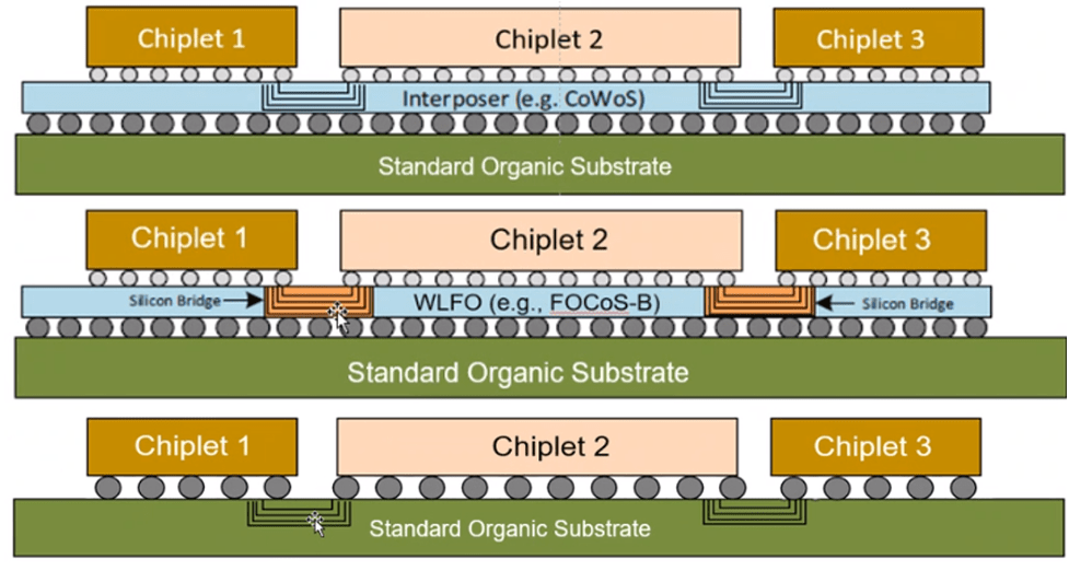
Fig 1. Chiplet interconnection for various substrate configurations. Source: Eliyan
When talking about an interposer, it generally is considered to be silicon. “The interposer could be a large piece of silicon (Fig 1 top), or just silicon bridges between the chips (Fig 1 middle) to provide the connectivity,” says Eliyan’s Farjadrad. “Both of these solutions use micro-bumps, which have high density. Interposers and bridges provide a lot of high-density bumps and traces, and that gives you bandwidth. If you utilize 1,000 wires each running at 5Gb, you get 5Tb. If you have 10,000, you get 50Tb. But those signals cannot go more than two or three millimeters. Alternatively, if you avoid the silicon interposer and you stay with an organic package (Fig 1 bottom), such as flip chip package, the density of the traces is 5X to 10X less. However, the thickness of the wires can be 5X to 10X more. That’s a significant advantage, because the resistance of the wires will go down by the square of the thickness of the wires. The cross section of that wire goes up by the square of that wire, so the resistance comes down significantly. If it’s 5X less density, that means you can run signals almost 25X further.”
For some people, it is all about bandwidth per millimeter. “If you have a parallel bus, or a parallel interface that is high speed, and you want bandwidth per millimeter, then you would probably pick a silicon interposer,” says Kent Stahn, senior manager of hardware engineering in Synopsys‘ Solutions Group. “An organic substrate is low-loss, low-cost, but it doesn’t have the density. In between, there are a bunch of solutions that deliver on some of that, but not for the same cost.”
There are other reasons to pick a substrate material, as well. “Silicon interposer comes from a foundry, so availability is a problem,” says Manuel Mota, senior staff product manager in Synopsys’ Solutions Group. “Some companies are facing challenges in sourcing advanced packages because capacity is taken. By going to other technologies that have a little less bandwidth density, but perhaps enough for your application, you can find them elsewhere. That’s becoming a critical aspect.”
All of these technologies are progressing rapidly, however. “The reticle limit is about 858mm square,” says Park. “People are talking about interposers that are perhaps four times that size, but we have laminates that go much bigger. Some of the laminate substrates coming from Japan are approaching that same level of interconnect density that we can get from silicon. I personally see more push towards organic substrates. Chip-on-Wafer-on-Substrate (CoWoS) from TSMC uses a silicon interposer and has been the technology of choice for about 12 years. More recently they introduced CoWoS-R, which uses film polyamide, closer to an organic type of substrate. Now we hear a lot about glass substrates.”
Over time, the total real estate inside the package may grow. “It doesn’t make sense for foundries to continue to build things the size of a 30-inch printed circuit board,” adds Park. “There are materials that are capable of addressing the bigger designs. Where we really need density is die-to-die. We want those chiplets right next to each other, a couple of millimeters of interconnect length. We want things very short. But the rest of it is just fanning out the I/O so that it connects to the PCB.”
This is why bridges are popular. “We do see a progression to bridges for the high-speed part of the interface,” say Synopsys’ Stahn. “The back side of it would be fanout, like RDL fanout. We see RDL packages that are going to be more like traditional packages going forward.”
Interposers offer additional capabilities. “Today, 99% of the interposers are passive,” says Park. “There’s no front end of line, there are no device layers. It’s purely back end of line processing. You are adding three, four, five metal layers to that silicon. That’s what we call a passive interposer. It’s just creating that die-to-die interconnect. But there are people taking that die and making it an active interposer, basically adding logic to that.”
That can happen for different purposes. “You already see some companies doing active interposers, where they add power management or some of the controls logic,” says Mota. “When you start putting active circuits on interposer, is it still a 2.5D integration, or does it become a 3D integration? We don’t see a big trend toward active interposers today.”
There are some new issues, though. “You have to consider coefficients of thermal expansion (CTE) mismatches,” says Stahn. “This happens whenever two materials with different CTEs are bonded together. Let’s start with the silicon interposer. You can get higher wattage systems, where the SoCs can be talking to their peers, and that can consume a lot of power. A silicon interposer still has to go in a package. The CTE mismatches are between the silicon to the package material. And with the bridge, you’re using it where you need it, but it’s still silicon die-to-die. You have to do the thermal mechanical analysis to make sure that the power that you’re delivering, and the CTE mismatches that you have, result in a viable system.”
While signal lengths in theory can get longer, this poses some problems. “When you’re making those long connections inside a chip, you typically limit those routes to a couple of millimeters, and then you buffer it,” says Mastroianni. “The problem with a passive silicon interposer is there are no buffers. That can really become a serious issue. If you do need to make those connections, you need to plan those out very carefully. And you do need to make sure you’re running timing analysis. Typically, your package guys are not going to be doing that analysis. That’s more of a problem that’s been solved with static timing analysis by silicon engineers. We do need to introduce an STA flow and deal with all the extractions that include organic and silicon type traces, and it becomes a new problem. When you start getting into some of those very long traces, your simple RC timing delays, which are assumed in normal STA delay calculators, don’t account for some of the inductance and mutual inductance between those traces, so you can get serious accuracy issues for those long traces.”
Active interposers help. “With active interposers, you can overcome some of the long-distance problems by putting in buffers or signal repeaters,” says Swinnen. “Then it starts looking more like a chip again, and you can only do it on silicon. You have the EMIB technology from Intel, where they embedded chiplet into the interposer and that’s an active bridge. The chip talks to the EMIB chip, and they both talk to you through this little active bridge chip, which is not exactly an active interposer, but acts almost like an active interposer.”
But even passive components add value. “The first thing that’s being done is including trench capacitors in the interposer,” says Mastroianni. “That gives you the ability to do some good decoupling, where it counts, close to the die. If you put them out on the board, you lose a lot of the benefits for the high-speed interfaces. If you can get them in the interposer, sitting right under where you have the fast-switching speed signals, you can get some localized decoupling.”
In addition to different materials, there is the question of who designs the interposer. “The industry seems to think of it as a little PCB in the context of who’s doing the design,” says Matt Commens, senior manager for product management at Ansys. “The interposers are typically being designed by packaging engineers, even though they are silicon processes. This is especially true for the high-performance ones. It seems counterintuitive, but they have that signal integrity background, they’ve been designing transmission lines and minimizing mismatch at interconnects. A traditional IC designer works from a component point of view. So certainly, the industry is telling us that the people they’re assigning to do that design work are packaging type of personas.”
Power
There are some considerable differences in routing between PCBs and interposers. “Interposer routing is much easier, as the number of components is drastically reduced compared to the PCB,” says Andy Heinig, head of department for efficient electronics at Fraunhofer IIS/EAS. “On the other hand, the power grid on the interposer is much more complex due to the higher resistance of the metal layers and the fact that the power grid is cut out by signal wires. The routing for the die-to-die interface is more complex due to the routing density.”
Power delivery looks very different. “If you look at a PCB, they put these big metal pour areas embedded in the layers, and they void out areas where things need to go through,” says Park. “You put down a bunch of copper and then you void out the others. We can’t build an interposer that way. We have to deposit the interconnect, so the power and ground structures on a silicon interposer will look more like a digital chip. But the signal will look more like a PCB or laminate package.”
Routing does look more like a PCB than a chip. “You’ll see things like teardrops or fillets where it makes a connection to a pad or via to create better yield,” adds Park. “The routing styles today are more aligned to PCBs than they are to a digital IC, where you just have 90° orthogonal corners and clean routing channels. For interposers, whether it’s silicon or organic, the via is often bigger than the wire, which is a classic PCB problem. The routers, if we’re talking about digital, is again more like a small PCB than a die.”
TSVs can create problems, too. “If you’re going to treat them as square, you’re losing a lot of space at the corners,” says Swinnen. “You really want 45° around those objects. Silicon routers are traditionally Manhattan, although there has been a long tradition of RDL routing, which is the top layer where the bumps are connected. That has traditionally used octagonal bumps or round bumps, and then 45° routing. It’s not as flexible as the PCB routing, but they have redistribution layer routers, and also they have some routers that come from the full custom side which have full river routing.”
- SEO Powered Content & PR Distribution. Get Amplified Today.
- PlatoData.Network Vertical Generative Ai. Empower Yourself. Access Here.
- PlatoAiStream. Web3 Intelligence. Knowledge Amplified. Access Here.
- PlatoESG. Carbon, CleanTech, Energy, Environment, Solar, Waste Management. Access Here.
- PlatoHealth. Biotech and Clinical Trials Intelligence. Access Here.
- Source: https://semiengineering.com/2-5d-integration-big-chip-or-small-pcb/

