As semiconductor devices become more complex, so do the methods for patterning them. Ever-smaller features at each new node require continuous advancements in photolithography techniques and technologies.
While the basic lithography process hasn’t changed since the founding of the industry — exposing light through a reticle onto a prepared silicon wafer — the techniques and technology of every part of that process have changed dramatically. These advancements have accelerated over the past five years as extreme ultraviolet (EUV) lithography transitioned from the lab into high-volume production at 7nm and 5nm. Now, with high-numerical-aperture (high-NA) EUV on the horizon, the debate between single patterning and multi-patterning techniques for 3nm nodes and below has intensified.
“EUV multi-patterning lithography has been unique in that decisions about whether to use single- or multi-patterning have needed to consider the required dose to expose a wafer and still be manufacturable,” says Kevin Lucas, senior architect for mask solutions at Synopsys. “A single-patterning lithography process may be more expensive than a double-patterning process, as single patterning may require more than twice the exposure dose, and have worse throughput on a very expensive scanner than a double-patterning process.”
Pushing the limits of single patterning
Single patterning involves using a single exposure step to create the desired patterns on a wafer, reducing the number of process steps and associated costs compared to multi-patterning methods. The technique has long been favored by semiconductor manufacturers for its simplicity and cost-effectiveness. Some of the benefits of single patterning include:
- Lower defect risk: With single patterning, there is a reduced risk of defects compared to multi-patterning, which can introduce alignment issues, overlay errors, and other defects that can compromise yield. By minimizing the number of process steps, single patterning inherently reduces these risks, resulting in higher yields and more reliable manufacturing outcomes.
- Enhanced throughput: Multi-patterning requires several lithography and etch cycles, each adding to the overall process time. In contrast, single patterning streamlines the manufacturing flow, allowing for faster processing of wafers.
- Lower Cost: Each additional exposure in multi-patterning necessitates additional masks and increased use of advanced lithography tools, driving up costs. By reducing the number of exposures needed, single patterning can lead to substantial savings in both materials and equipment usage.
- Simplified Process Control: Managing the process parameters and ensuring consistency across multiple exposures in multi-patterning can be challenging. Single patterning simplifies process control, making it easier to maintain uniformity and repeatability in the manufacturing process.
“Manufacturers work really hard to make single patterning work because nobody wants to do double patterning,” says Chris Mack, CTO of Fractilia. “It’s just too expensive, so that’s exactly what has happened in the last five years. Companies have pushed as hard as they could on single-patterning technology and delayed the need for double patterning longer than anyone anticipated.”
Incremental improvements in the quality of EUV scanners have played a crucial role in extending single patterning beyond what was possible five years ago, when the ASML NXE:3400C scanner was just being introduced. Since then, further advancements in power and scanner technology, including better lenses and more sophisticated illuminators, have contributed to lower defect rates and higher yields. These improvements have enhanced the practical resolution achievable with single patterning, making it a more viable option for smaller features.
“ASML has come out with a succession of models of their 0.33 NA EUV lithography equipment, and each time they do, it has a bit more throughput, a little better overlay, the lenses are better,” says Harry Levinson, principal lithographer at HJL Lithography. “They started with the 3300, then we got the 3350, 3400, and 3600. Now they’re shipping 3800s, and with each one, the reliability keeps improving.”
The higher source power of ASML’s latest EUV equipment enables the use of higher doses, which in turn improves resolution and reduces the likelihood of defects. Additionally, advancements in new photoresist technology have enhanced sensitivity and resolution, allowing for more precise patterning at smaller pitches.
“In addition to improving the spec of the EUV scanner itself, similar tricks that were used in 193nm dry and immersion have been applied to EUV to support tighter pitches,” says Dr. Leo Pang, chief product officer and executive vice president at D2S. “Many of those are resolution enhancement techniques (RET), source and mask optimization (SMO), more aggressive optical proximity correction (OPC) and even curvilinear OPC, plus inverse lithography technology (ILT), both Manhattanized and curvilinear, for hot spots.”
What used to be challenging at 32nm pitches became a challenge at 30nm, and what was challenging at 30nm is now becoming manageable at 28nm. Although achieving real 28-nanometer pitches using single patterning is still difficult, the improvements in EUV tools and resist capabilities have brought us close.
But popular as it is, single patterning has its drawbacks. At smaller nodes, single patterning has difficulty achieving finer pitches with high precision. As feature sizes shrink, that margin for error decreases, making it harder to maintain pattern fidelity and control defects. The stochastic nature of photon absorption in photoresists at these scales can also lead to variations that result in defects, which are more problematic as the critical dimensions shrink. Additionally, the higher doses required for single patterning at these smaller pitches can significantly increase the overall process cost and reduce throughput.
“Manufacturers want to push single patterning as low as it can go, because it’s more cost-effective,” says Mack. “But it’s not always that easy, because to make single patterning provide good yield often requires a higher imaging dose, and that higher dose adds cost. Now you’ve got a higher-cost single patterning compared to a higher-cost double patterning, and it can get tricky knowing exactly where the tradeoff is.”
Multi-patterning
While single patterning offers several advantages, it also has inherent limitations that become more pronounced at smaller nodes. As feature sizes continue to shrink, the industry has increasingly turned to multi-patterning techniques to achieve the necessary precision and fidelity to pattern the smallest features at advanced nodes like 3nm and below.
“Double patterning is inherently more complex and expensive than single patterning, but it’s essential for achieving the smallest features at advanced nodes,” says Levinson. “It requires multiple hard masks and multiple exposures (see figure 1), but if you have a loose pitch and you’re doing double patterning, you can use a lower dose, which means each layer has higher throughput than with a single exposure. So there’s a little offsetting of the cost.”
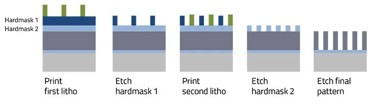
Fig. 1: Double patterning increases density. Source: Lam Research
The industry has practiced multiple patterning with immersion lithography for many years, accumulating a vast amount of knowledge about decomposing design layouts and self-aligned processes. The principles of multi-patterning remain the same, whether for 193 immersion or EUV, but achieving the required levels of process control and precision necessary to achieve yield goals at 3nm nodes and below requires new strategies.
Process control and AI
One of the significant challenges with multi-patterning is managing the multiple exposures and ensuring the overall performance of the resulting patterns meets the required specifications. Multiple exposures add control difficulties, making it harder to maintain pattern fidelity and consistency. Moreover, using these techniques with expensive EUV tools further complicates the cost trade-off.
“Advanced lithography has well over 1,000 equipment and process parameters that need to be characterized and monitored for quality outcomes,” says Boyd Finlay, director of solutions engineering at Tignis. “This need is accelerating EUV development cycles for artificial intelligence (AI) systems capable of optimizing multi-patterning lithography and improving process issues like overlay error at these advanced nodes.”
Additionally, multi-patterning techniques like self-aligned double patterning (SADP) and self-aligned quadruple patterning (SAQP) are necessary for producing the fine features required at 3nm and below.
Self-aligned double patterning (SADP) involves creating a pattern by using a single lithographic exposure followed by a series of deposition and etch steps. The process typically begins with the deposition of a spacer material on the sides of a pre-patterned feature. This spacer is then used as a mask for subsequent etching steps, effectively doubling the number of features originally patterned by the single exposure.
“An SADP EUV process can also take advantage of EUV’s high lithographic resolution to create very tight line-end spaces and other area-saving features desired by designers,” says Lucas. “However, advanced manufacturing tools such as inverse lithography technology (ILT) are needed that can highly optimize the mask pattern to reduce the minimum size and spaces between circuit features on the wafer.”
Self-aligned quadruple patterning (SAQP) extends the principles of SADP to achieve even smaller feature sizes. SAQP involves additional cycles of spacer deposition and etching, effectively quadrupling the pattern density from the original lithographic exposure. This method is particularly useful for creating extremely fine pitches required at nodes like 3nm and below.
“The industry has practiced multiple patterning with immersion lithography for many years,” says Levinson. “There has been a tremendous amount of learning, particularly in decomposing design layouts and developing self-aligned processes. Many of these techniques and lessons can be re-used with EUV lithography. It’s not that there are any new tricks with EUV. Rather, as we move to smaller dimensions, the need for heightened levels of process control and precision becomes even more critical.”
EUV mask innovations
Over the past five years, the infrastructure and techniques for EUV mask-making have improved significantly to meet the stringent requirements of the 7nm and 5nm nodes. The adoption of EUV lithography has driven developments in optical proximity correction (OPC) and ILT, which are critical for managing data volumes and ensuring precise inspection of EUV mask features.
ASML also has made significant strides in enhancing the EUV pellicle, achieving transmission rates of 83% to 84%, which has notably improved overall defectivity and transmission accuracy. The quality of EUV masks overall has improved, as well, making EUV lithography more viable for high-volume manufacturing.
“It seems that Hoya and Asahi Glass are now making enough defect-free mask blanks that people can actually consider exposing with certain types of masks,” says Levinson. “This was unthinkable just a few years ago.” This improvement in defect-free mask blanks is remarkable, considering that it was only five years ago when producing a single EUV mask blank without defects was a significant milestone.
Curvilinear masking and multi-patterning
Curvilinear masking has gained significant attention for its potential to enhance device performance and reduce power consumption. Curvilinear features allow for more efficient designs, leading to higher performance and lower power consumption in the final devices. However, integrating curvilinear features into multi-patterning processes is a long way off. The computational complexity of designing curvilinear masks already requires GPU acceleration and AI support, and that complexity increases exponentially with multiple patterning.
“Curvilinear mask patterns were initially driven by curvilinear ILT to gain the best resolution and process window and were enabled by multi-beam mask writers. Since all EUV masks are written by multi-beam mask writers, they can also be curvilinear,” says D2S’ Pang. “OPC in particular is easily extended from segment-based Manhattan OPC to control point based curvilinear OPC, and companies are busy applying curvilinear masks to both EUV and DUV layers to shrink the node and improve the yield. The next requirement the industry faces is the need to extend ILT to full chip or full slit curvilinear ILT for EUV. Once there is an ILT product that can do full slit curvilinear ILT for EUV, it will be adopted by the industry.”
One approach to managing these complexities may be to keep the stitching boundary as simple as possible, with minimally complicated features in the boundary itself and more complex curvilinear features in the half-size reticles similar to the approach taken in multichip modules. This method helps maintain alignment and overlay accuracy, which are critical for the success of multi-patterning at advanced nodes. It ensures that critical features are not compromised during the stitching process, maintaining the integrity and performance of the final device.
“Even if it’s possible, it will take a while to work out the solutions for multiple patterning with curvilinear features,” Levinson noted. “The physics of lithography at these scales, including managing 3D effects and non-monochromatic light sources, adds huge layers of complexity to the process.”
High-NA EUV
The introduction of high-NA EUV lithography in the next few years is poised to significantly influence the patterning landscape by offering higher resolution and improved pattern fidelity. High-NA EUV technology aims to reduce the need for multi-patterning, extending single patterning to 3nm and beyond. However, transitioning to high-NA EUV brings its own set of challenges, requiring substantial technical and financial investment.
The main advantage of high-NA EUV is its ability to achieve finer resolutions, pushing the boundaries of semiconductor manufacturing into the angstrom era. However, this increased resolution brings new challenges, particularly in managing stochastic effects and developing new resist materials capable of withstanding higher doses when patterning a thinner layer.
“For the 14 angstrom and 10 angstrom nodes, the industry will use high-NA EUV, which requires double exposure stitching to manufacture large chip sizes,” says Synopsys’ Lucas. “High-NA EUV will require innovative solutions for stitching and overlay control, as well as advanced resist materials to cope with the tighter process windows.”
One of the primary challenges with high-NA EUV is the development of suitable resist materials, primarily metal oxides. This shift from traditional chemically amplified resists to metal oxide resists is a significant change for the industry. While metal oxide resists offer improved performance at smaller nodes due to their higher resolution and sensitivity, they are not yet ready for mass production.
Nevertheless, high-NA EUV technology is progressing faster than expected. “It’s really quite remarkable that they are imaging with these tools this summer,” says Fractilia’s Mack. “But the high initial investment for high-NA EUV infrastructure is a significant barrier, not to mention the ongoing costs of operation. Companies will have to weigh these costs against the potential benefits.”
Conclusion
The past five years have seen remarkable progress in EUV lithography, particularly in the areas of single and double patterning. These advancements are essential to enabling the production of advanced semiconductor devices at smaller nodes. As the industry moves toward the adoption of high-NA EUV tools, continued innovation and collaboration will be essential to overcome new challenges and realize the full potential of these cutting-edge technologies.
The ongoing debate between single and multi-patterning in EUV lithography underscores the dynamic nature of semiconductor manufacturing. At 3nm node and beyond, both methods will play critical roles, shaped by technological advancements and economic considerations.
Related Reading
Big Changes Ahead For Photomask Technology
Curvilinear technology could boost yield and improve scalability, but it requires full industry support and a lot of work.
- SEO Powered Content & PR Distribution. Get Amplified Today.
- PlatoData.Network Vertical Generative Ai. Empower Yourself. Access Here.
- PlatoAiStream. Web3 Intelligence. Knowledge Amplified. Access Here.
- PlatoESG. Carbon, CleanTech, Energy, Environment, Solar, Waste Management. Access Here.
- PlatoHealth. Biotech and Clinical Trials Intelligence. Access Here.
- Source: https://semiengineering.com/single-vs-multi-patterning-advancements-for-euv/

