Chiplets are gaining renewed attention in the automotive market, where increasing electrification and intense competition are forcing companies to accelerate their design and production schedules.
Electrification has lit a fire under some of the biggest and best-known carmakers, which are struggling to remain competitive in the face of very short market windows and constantly changing requirements. Unlike in the past, when carmakers typically ran on five- to seven-year design cycles, the latest technology in vehicles today may well be considered dated within several years. And if they cannot keep up, there is a whole new crop of startups producing cheap vehicles with the ability to update or change out features as quickly as a software update.
But software has speed, security, and reliability limitations, and being able to customize the hardware is where many automakers are now putting their efforts. This is where chiplets fit in, and the focus now is on how to build enough interoperability across large ecosystems to make this a plug-and-play market. The key factors to enable automotive chiplet interoperability include standardization, interconnect technologies, communication protocols, power and thermal management, security, testing and ecosystem collaboration.
Similar to non-automotive applications at the board level, many design efforts are focusing on a die-to-die approach, which is driving a number of novel design considerations and tradeoffs. At the chip level, the interconnects between various processors, chips, memory, and I/O are becoming more complex due to increased design performance requirements, spurring a flurry of standards activities. Different interconnect and interface types have been proposed to serve varying purposes, while emerging chiplet technologies for dedicated functions — processors, memories, and I/Os, to name a few — are changing the approach to chip design.
“There is a realization by automotive OEMs that to control their own destiny, they’re going to have to control their own SoCs,” said David Fritz, vice president of virtual and hybrid systems at Siemens EDA. “However, they don’t understand how far along EDA has come since they were in college in 1982. Also, they believe they need to go to the latest process node, where a mask set is going to cost $100 million. They can’t afford that. They also don’t have access to talent because the talent pool is fairly small. With all that together comes the realization by the OEMs that to control their destiny, they need a technology that’s developed by others, but which can be combined however needed to have a unique differentiated product they are confident is future-proof for at least a few model years. Then it becomes economically viable. The only thing that fits the bill is chiplets.”
Chiplets can be optimized for specific functions, which can help automakers meet reliability, safety, security requirements with technology that has been proven across multiple vehicle designs. In addition, they can shorten time to market and ultimately reduce the cost of different features and functions.
Demand for chips has been on the rise for the past decade. According to Allied Market Research, global automotive chip demand will grow from $49.8 billion in 2021 to $121.3 billion by 2031. That growth will attract even more automotive chip innovation and investment, and chiplets are expected to be a big beneficiary.
But the marketplace for chiplets will take time to mature, and it will likely roll out in phases. Initially, a vendor will provide different flavors of proprietary dies. Then, partners will work together to supply chiplets to support each other, as has already happened with some vendors. The final stage will be universally interoperable chiplets, as supported by UCIe or some other interconnect scheme.
Getting to the final stage will be the hardest, and it will require significant changes. To ensure interoperability, large enough portions of the automotive ecosystem and supply chain must come together, including hardware and software developers, foundries, OSATs, and material and equipment suppliers.
Momentum is building
On the plus side, not all of this is starting from scratch. At the board level, modules and sub-systems always have used onboard chip-to-chip interfaces, and they will continue to do so. Various chip and IP providers, including Cadence, Diode, Microchip, NXP, Renesas, Rambus, Infineon, Arm, and Synopsys, provide off-the-shelf interface chips or IP to create the interface silicon.
The Universal Chiplet Interconnect Express (UCIe) Consortium is the driving force behind the die-to-die, open interconnect standard. The group released its latest UCIe 1.1 specification in August 2023. Board members include Alibaba, AMD, Arm, ASE, Google Cloud, Intel, Meta, Microsoft, NVIDIA, Qualcomm, and Samsung, and others. Industry partners are showing widespread support. AIB and Bunch of Wires (BoW) also have been proposed. In addition, Arm just released its own Chiplet System Architecture, along with an updated AMBA spec to standardize protocols for chiplets.
“Chiplets are already here, driven by necessity,” said Arif Khan, senior product marketing group director for design IP at Cadence. “The growing processor and SoC sizes are hitting the reticle limit and the diseconomies of scale. Incremental gains from process technology advances are lower than rising cost per transistor and design. The advances in packaging technology (2.5D/3D) and interface standardization at a die-to-die level, such as UCIe, will facilitate chiplet development.”
Nearly all of the chiplets used today are developed in-house by big chipmakers such as Intel, AMD, and Marvell, because they can tightly control the characteristics and behavior of those chiplets. But there is work underway at every level to open this market to more players. When that happens, smaller companies can begin capitalizing on what the high-profile trail blazers have accomplished so far, and innovating around those developments.
“Many of us believe the dream of having an off-the-shelf, interoperable chiplet portfolio will likely take years before becoming a reality,” said Guillaume Boillet, senior director strategic marketing at Arteris, adding that interoperability will emerge from groups of partners who are addressing the risk of incomplete specifications.
This also is raising the attractiveness of FPGAs and eFPGAs, which can provide a level of customization and updates for hardware in the field. “Chiplets are a real thing,” said Geoff Tate, CEO of Flex Logix. “Right now, a company building two or more chiplets can operate much more economically than a company building near-reticle-size die with almost no yield. Chiplet standardization still appears to be far away. Even UCIe is not a fixed standard yet. Not all agree on UCIe, bare die testing, and who owns the problem when the integrated package doesn’t work, etc. We do have some customers who use or are evaluating eFPGA for interfaces where standards are in flux like UCIe. They can implement silicon now and use the eFPGA to conform to standards changes later.”
There are other efforts supporting chiplets, as well, although for somewhat different reasons — notably, the rising cost of device scaling and the need to incorporate more features into chips, which are reticle-constrained at the most advanced nodes. But those efforts also pave the way for chiplets in automotive, and there is strong industry backing to make this all work. For example, under the sponsorship of SEMI, ASME, and three IEEE Societies, the new Heterogeneous Integration Roadmap (HIR) looks at various microelectronics design, materials and packaging issues to come up with a roadmap for the semiconductor industry. Their current focus includes 2.5D, 3D-ICs, wafer-level packaging, integrated photonics, MEMS and sensors, and system-in-package (SiP), aerospace, automotive, and more.
At the recent Heterogeneous Integration Global Summit 2023, representatives from AMD, Applied Materials, ASE, Lam Research, MediaTek, Micron, Onto Innovation, TSMC, and others demonstrated strong support for chiplets. Another group that supports chiplets is the Chiplet Design Exchange (CDX) working group , which is part of the Open Domain Specific Architecture (ODSA) and the Open Compute Project Foundation (OCP). The Chiplet Design Exchange (CDX) charter focuses on the various characteristics of chiplet and chiplet integration, including electrical, mechanical, and thermal design exchange standards of the 2.5D stacked, and 3D Integrated Circuits (3D-ICs). Its representatives include Ansys, Applied Materials, Arm, Ayar Labs, Broadcom, Cadence, Intel, Macom, Marvell, Microsemi, NXP, Siemens EDA, Synopsys, and others.
“The things that automotive companies want in terms of what each chiplet does in terms of functionality is still in an upheaval mode,” Siemens’ Fritz noted. “One extreme has these problems, the other extreme has those problems. This is the sweet spot. This is what’s needed. And these are the types of companies that can go off and do that sort of work, and then you could put them together. Then this interoperability thing is not a big deal. The OEM can make it too complex by saying, ‘I have to handle that whole spectrum of possibilities.’ The alternative is that they could say, ‘It’s just like a high speed PCIe. If I want to communicate from one to the other, I already know how to do that. I’ve got drivers that are running my operating system. That would solve an awful lot of problems, and that’s where I believe it’s going to end up.”
One path to universal chiplet development?
Moving forward, chiplets are a focal point for both the automotive and chip industries, and that will involve everything from chiplet IP to memory interconnects and customization options and limitations.
For example, Renesas Electronics announced in November 2023 plans for its next-generation SoCs and MCUs. The company is targeting all major applications across the automotive digital domain, including advance information about its fifth-generation R-Car SoC for high-performance applications with advanced in-package chiplet integration technology, which are meant to provide automotive engineers greater flexibility to customize their designs.
Renesas noted that if more AI performance is required in Advanced Driver Assistance Systems (ADAS), engineers will have the capability to integrate AI accelerators into a single chip. The company said this roadmap comes after years of collaboration and discussions with Tier 1 and OEM customers, which have been clamoring for a way to accelerate development without compromising quality, including designing and verifying the software even before the hardware is available.
“Due to the ever increasing needs to increase compute on demand, and the increasing need for higher levels of autonomy in the cars of tomorrow, we see challenges in monolithic solutions scaling and providing the performance needs of the market in the upcoming years,” said Vasanth Waran, senior director for SoC Business & Strategies at Renesas. “Chiplets allows for the compute solutions to scale above and beyond the needs of the market.”
Renesas announced plans to create a chiplet-based product family specifically targeted at the automotive market starting in 2025.
Standard interfaces allow for SoC customization
It is not entirely clear how much overlap there will be between standard processors, which is where most chiplets are used today, and chiplets developed for automotive applications. But the underlying technologies and developments certainly will build off each other as this technology shifts into new markets.
“Whether it is an AI accelerator or ADAS automotive application, customers need standard interface IP blocks,” noted David Ridgeway, senior product manager, IP accelerated solutions group at Synopsys. “It is important to provide fully verified IP subsystems around their IP customization requirements to support the subsystem components used in the customers’ SoCs. When I say customization, you might not realize how customizable IP has become over the course of the last 10 to 20 years, on the PHY side as well as the controller side. For example, PCI Express has gone from PCIe Gen 3 to Gen 4 to Gen 5 and now Gen 6. The controller can be configured to support multiple bifurcation modes of smaller link widths, including one x16, two x8, or four x4. Our subsystem IP team works with customers to ensure all the customization requirements are met. For AI applications, signal and power integrity is extremely important to meet their performance requirements. Almost all our customers are seeking to push the envelope to achieve the highest memory bandwidth speeds possible so that their TPU can process many more transactions per second. Whenever the applications are cloud computing or artificial intelligence, customers want the fastest response rate possible.”
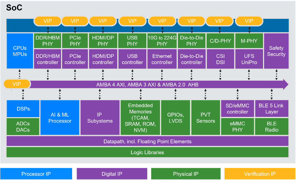
Fig 1: IP blocks including processor, digital, PHY, and verification help developers implement the entire SoC. Source: Synopsys
Optimizing PPA serves the ultimate goal of increasing efficiency, and this makes chiplets particularly attractive in automotive applications. When UCIe matures, it is expected to improve overall performance exponentially. For example, UCIe can deliver a shoreline bandwidth of 28 to 224 GB/s/mm in a standard package, and 165 to 1317 GB/s/mm in an advanced package. This represents a performance improvement of 20- to 100-fold. Bringing latency down from 20ns to 2ns represents a 10-fold improvement. Around 10 times greater power efficiency, at 0.5 pJ/b (standard package) and 0.25 pJ/b (advanced package), is another plus. The key is shortening the interface distance whenever possible.
To optimize chiplet designs, the UCIe Consortium provides some suggestions:
- Careful planning consideration of architectural cut-lines (i.e. chiplet boundaries), optimizing for power, latency, silicon area, and IP reuse. For example, customizing one chiplet that needs a leading-edge process node while re-using other chiplets on older nodes may impact cost and time.
- Thermal and mechanical packaging constraints need to be planned out for package thermal envelopes, hot spots, chiplet placements and I/O routing and breakouts.
- Process nodes need to be carefully selected, particularly in the context of the associated power delivery scheme.
- Test strategy for chiplets and packaged/assembled parts need to be developed up front to ensure silicon issues are caught at the chiplet-level testing phase rather than after they are assembled into a package.
Conclusion
The idea of standardizing die-to-die interfaces is catching on quickly but the path to get there will take time, effort, and a lot of collaboration among companies that rarely talk with each other. Building a vehicle takes one determine carmaker. Building a vehicle with chiplets requires an entire ecosystem that includes the developers, foundries, OSATs, and material and equipment suppliers to work together.
Automotive OEMs are experts at putting systems together and at finding innovative ways to cut costs. But it remains to seen how quickly and effectively they can build and leverage an ecosystem of interoperable chiplets to shrink design cycles, improve customization, and adapt to a world in which the leading edge technology may be outdated by the time it is fully designed, tested, and available to consumers.
— Ann Mutschler contributed to this report.
- SEO Powered Content & PR Distribution. Get Amplified Today.
- PlatoData.Network Vertical Generative Ai. Empower Yourself. Access Here.
- PlatoAiStream. Web3 Intelligence. Knowledge Amplified. Access Here.
- PlatoESG. Carbon, CleanTech, Energy, Environment, Solar, Waste Management. Access Here.
- PlatoHealth. Biotech and Clinical Trials Intelligence. Access Here.
- Source: https://semiengineering.com/why-chiplets-are-so-critical-in-automotive/

