Chipmakers are utilizing both evolutionary and revolutionary technologies to achieve orders of magnitude improvements in performance at the same or lower power, signaling a fundamental shift from manufacturing-driven designs to those driven by semiconductor architects.
In the past, most chips contained one or two leading-edge technologies, mostly to keep pace with the expected improvements in lithography at each new process node every couple of years. Those improvements were based on industry roadmaps that called for predictable but unremarkable gains over time. Now, with the explosion in data fueled by large language models and more sensors — as well as increased competition between systems companies designing their own chips, and growing international rivalries involving AI — the rules are changing rather dramatically at the leading edge of chip design. Incremental improvements now are being coupled with giant leaps in processing performance, and while those enable a whole new level of compute capabilities and analytics, they also require a whole new set of tradeoffs.
At the heart of these shifts are highly customized chip architectures, some involving chiplets developed at the most advanced process nodes. Parallel processing is almost a given, and so are accelerators aimed at specific data types and operations. In some cases, these mini-systems will not be sold commercially because they are what gives data centers their competitive edge. But they also may include other commercially available technology, such as processing cores or accelerators or in- or near-memory compute technology to reduce latency, as well as different caching schemes, co-packaged optics, and much faster interconnects. Many of these developments have been in research or sitting on the sidelines for years, and they are now being fully deployed.
Amin Vahdat, engineering fellow and vice president for ML systems at Google Research, noted in a presentation at the recent Hot Chips 2023 conference that chips today can take on problems that were unthinkable a decade ago, and that machine learning will take up an “increasing fraction” of compute cycles.
“We need to change how we look at system design,” Vahdat said. “The rise in computing demand over the past five, six, seven years has been stunning … While a lot of innovations are coming in terms of [algorithm] sparsity, when you’re looking at [figure 1, below], it shows 10X a year, sustained, in the number of parameters per model. And we also know that the computation costs grow super-linearly with the number of parameters. So the kind of computing infrastructure that we have to build to meet this challenge has to change. It’s important to note that we would not be where we are today if we tried to do this on general-purpose compute. The conventional compute wisdom that we’ve developed over the past 50 or 60 years has been thrown out the window.”
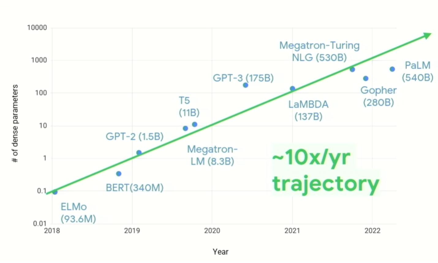
Fig. 1: Demand growth for ML compute. Source: Google Research/Hot Chips 2023
That doesn’t mean old problems disappear, however. Power and thermal dissipation are persistent headaches for design teams, and they become more difficult to resolve as the speed and amount of processing increases. Just turning up the clock frequency stopped being a straightforward option after about 3GHz due to higher thermal density and the inability of chips to dissipate that heat. And while sparse data models and hardware-software co-design address the efficiency of software running on various processing elements, as well as the ability to process more per compute cycle, there is no longer a single knob to turn to improve performance per watt.
Memory innovations
There are, however, lots of smaller and mid-sized knobs, some of which have never been used in production systems because there wasn’t an economic reason to do so. Those economics have changed dramatically with the increase in data and the shift to architectural innovation, which was readily evident at this year’s Hot Chips conference.
Among the options are in-memory/near-memory processing, as well as processing closer to the source of data. The issue here is that moving large volumes of data requires significant system resources — bandwidth, power, and time — which has a direct economic impact on computing. In general, much of the data collected and processed is useless. For instance, the relevant data in a video feed in a car or a security system may last only a second or two, while there may be hours of data to sort through. Pre-processing the data closer to the source, and using AI to identify the data of interest, means only a small fraction needs to be sent on for further processing and storage.
“Most of the energy consumption comes from moving data,” said Jin Hyun Kim, principal engineer at Samsung. He pointed to three solutions to improve efficiency and ratchet up performance:
- In-memory processing for extreme bandwidth and power, using HBM;
- In-memory processing for low-power devices that require high capacity, using LPDDR, and
- Near-memory processing using CXL for extreme capacity at a moderate cost.
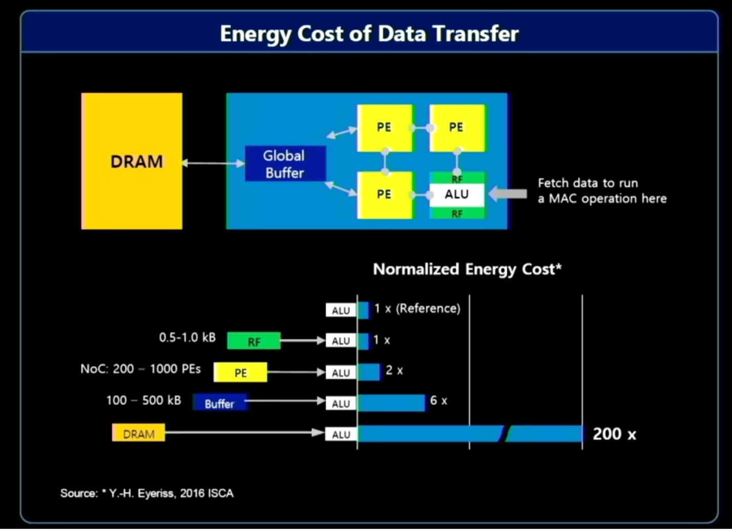

Fig. 2: Resource cost of moving data. Source: Samsung/Hot Chips 2023
In-memory processing has been on the drawing board for years, without much movement until very recently. Large language models have changed the economics so drastically that it now has become much more interesting, and that hasn’t been lost on large memory vendors.
A new refinement on this concept is in-memory acceleration, which is particularly useful for multiply and accumulate (MAC) functions for AI/ML, where the amount of data that needs to be processed quickly is exploding. With Generative Pre-Trained Transformer 3 (GPT-3) and GPT4, just loading the data requires massive bandwidth. There are multiple challenges associated with that, including how to do this efficiently while maximizing performance and throughput, how to scale it to handle rapid increases in the number of parameters in large language models, and how to build in flexibility to accommodate future changes.
“The mindset we had at the beginning is memory as an accelerator,” said Yonkwee Kwon, senior technical sensing manager at SK hynix America, in a presentation at Hot Chips 2023. “The first goal was to enable efficient scaling. But it’s also important to have high performance. And lastly, we designed the system architecture for ease of programming while minimizing system structure overhead, but still allowing a software stack for flexibility.
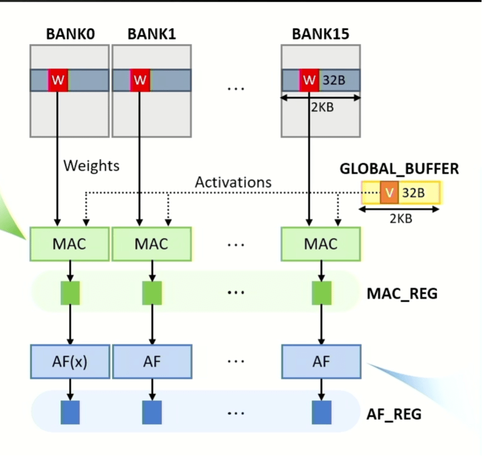

Fig. 3: MAC and activation operations can be performed in all banks in parallel, with weight matrix data sourced from banks and vector data sourced from global buffer. MAC and activation function results are stored in latches called MAC_REG and AF_REG, respectively. Source: SK hynix/Hot Chips 2023
CPU improvements
While changes in memory help reduce the amount of data that needs to be moved, that’s only one piece of the puzzle. The next challenge is to speed up the main processing elements. One way to do that is branch prediction, which basically predicts what the next operation will be — almost the way an internet search engine does. As with any parallelized architecture, though, the key is to keep various processing elements fully operating with no idle time in order to maximize performance and efficiency.
Arm is taking a new twist on this concept with its Neoverse V2 design, decoupling branch from fetch. The result is higher efficiency by minimizing stalls, and faster recovery from mispredictions. “Dynamic feed mechanisms allow the core to regulate aggressiveness, and proactively prevent system congestion,” said Magnus Bruce, lead CPU architect at Arm. “These fundamental concepts are what allow us to push width and depth of the machine while maintaining the short pipeline for quick mis-predict recovery.”

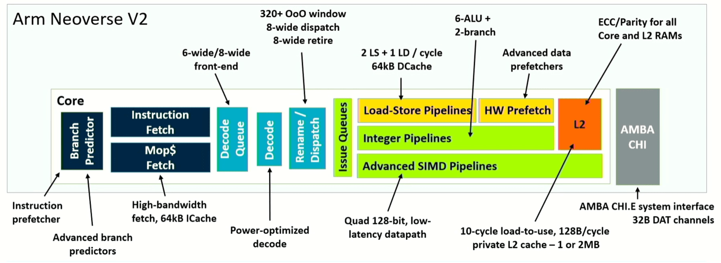
Fig. 4: Pipeline schematic of Neoverse V2 core. Source: Arm/Hot Chips 2023
What’s different here is the total system improvement comes from tweaks of the architecture at multiple points, rather than a wholesale change. For instance, splitting the branch predictor and fetch allows the branch target buffer to be split into two levels, enabling it to handle 50% more entries. It also triples the history stored in the predictor, and doubles the number of entries in the fetch queue, resulting in a significant real-world performance improvement. To make that effective, the architecture also doubles L2 cache, which separates out used-once and used-multiple data-block predictions. Adding up the various improvements, Neoverse V2 shows up to twice the performance of V1, depending upon what role it plays in a system.
AMD’s next-gen Zen 4 Core, meanwhile, increases instructions per cycle by about 14% due to microarchitectural improvements, offers 16% higher frequency at 5nm at the same voltage due to process scaling, and about 60% lower power due micro-architectural and physical design improvements.
Like Arm, AMD is focusing on improvements in branch prediction and fetch. Kai Troester, AMD fellow and lead architect of the Zen 4, said branch prediction accuracy increased due to more branches, more branch predictions per cycle, and a bigger operational cache that allows more entries and more operations per entry. It also adds a 3D V-cache, which boosts L3 cache per core to as much as 96 Mbytes, and provides support for 512-bit operations using two consecutive cycles on a 256-bit data path. In simple terms, the design increases the size of the data pipes, and whenever possible it shortens the distances the data must travel.
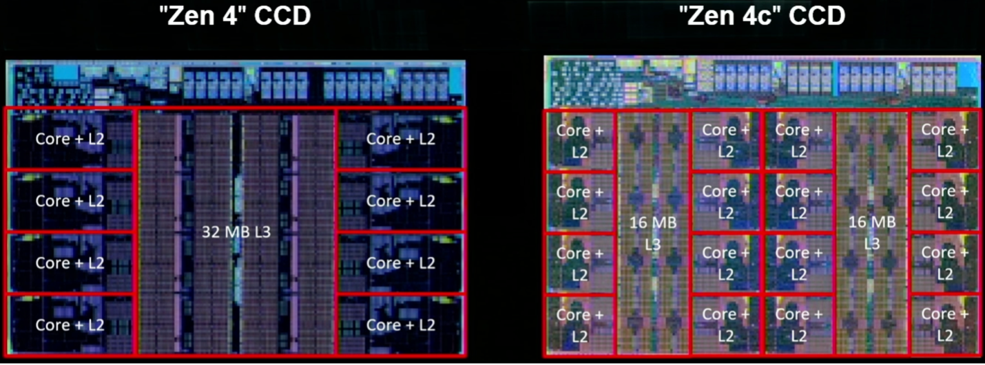

Fig. 5: Two implementations of Zen 4, including the Zen 4c with twice the number of compute cores per die and partitioned L3 cache. Source: AMD/Hot Chips 2023
Platform architectures
One of the key trends on the system side is increasing domain specificity, which has wreaked havoc on the old model of developing a general-purpose processor that works across all applications. The challenge now is how to deliver what is essentially mass customization, and there are two main approaches for that — adding programmability, either through hardware or programmable logic, and developing a platform for interchangeable parts.
Intel unveiled a framework for integrating chiplets into an advanced package that leverages its Embedded Multi-die Interconnect Bridge to connect high-speed I/O, processor cores, and memory. Intel’s goal has been to provide enough customization and performance to satisfy customers, but to deliver those systems much more quickly than fully customized architectures and with predictable results.
“This will be a multi-die architecture,” said Chris Gianos, Intel fellow and lead Xeon architect. “We have a lot of flexibility in the structure that we can build with these chiplets. They all just interoperate, and it gives us one of those dimensions to optimize the product cores specifically. And we’ll create chiplets that are E-cores (ultra-efficient) and chiplets that are P-cores (high-performance).”
Intel also created a modular mesh fabric to tie together various components, as well as a common controller that supports DDR or MCR memory and memory that is attached through CXL.

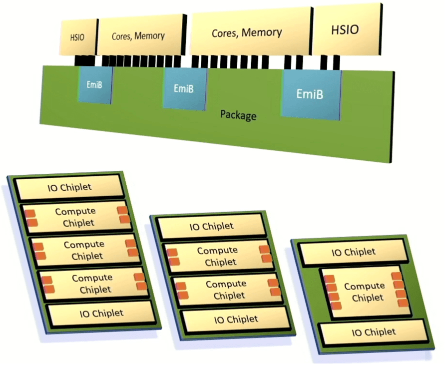
Fig. 6: Intel’s customizable chiplet architecture. The orange boxes represent memory channels. Source: Intel/Hot Chips 2023
Neural processors, optical interconnects
The list of new approaches and technologies is unprecedented, even for the Hot Chips conference. What it shows is just how widely the industry is searching for new ways to increase power and reduce power, while still keeping an eye on area and cost. PPAC remains the focus, but the tradeoffs for different applications and use cases can be very different.
“The OpEx and CapEx of AI are becoming unsustainable,” said Dharmendra Modha, IBM fellow, adding that “architecture trumps Moore’s Law.”
Also critical for AI/ML applications is precision. IBM’s design includes a vector matrix multiplier that allows for mixed precision, and vector compute units and activation function units with FP16 precision. In addition, processing is done within a few microns away from memory. “There is no data-dependent conditional branching,” he said. “There are no cache misses, no stalls, no speculative execution.”

Fig. 7: IBM’s North Pole chip, showing intertwined compute (red) and memory (blue). Source: IBM/Hot Chips 2023
A key challenge in complex chips is not just moving data between memory and processors, but all around the chip. Network-on-chip and other interconnect fabrics simplify this process. Silicon photonics has been in use for some time, particularly for high-speed networking chips, and photonics plays a role between servers in a rack. But whether, or when, it moves to the chip level remains uncertain. Nevertheless, work continues in this area, and based on numerous interviews across the chip industry, photonics is on the radar of many companies.
Maurice Steinman, vice president of engineering at Lightelligence, said his company has developed purpose-built photonics-based accelerators that are 100X faster than GPUs at significantly lower power. The company also has developed optical networks-on-chip, which are more about using silicon interposers as the medium for connecting chiplets using photons rather than electrons.
“The challenge with a purely electrical solution is that with the attenuation over distance, it really becomes practical to only do communication between nearest neighbors,” said Steinman. “If there’s a result in the top left [of a chip] that needs to communicate with the bottom right, it needs to traverse many hops. That creates a problem for the software components that are responsible for allocating resources, because it needs to think several chess moves ahead to avoid congestion.”
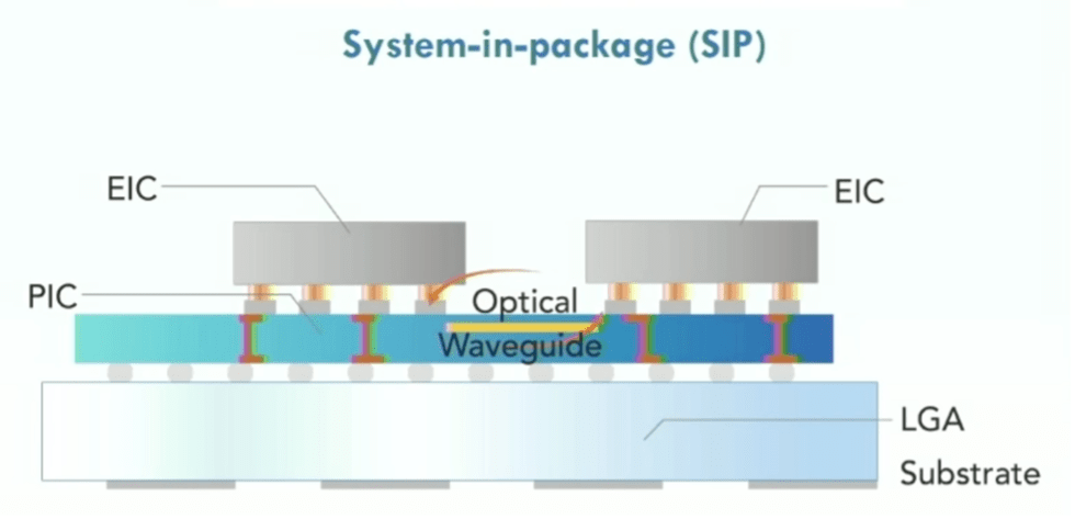

Fig. 8: Optical network on chip showing photonic integrated circuit (PIC), eletrical integrated circuits (EICs), using land grid array (LGA) substrate. Source: Lightelligence/Hot Chips 2023
Sustainability, reliability, and the future
With all of these changes, two other issues have emerged. One is sustainability. As more data is processed by more chips, the challenge will be staying even on energy consumption, let alone reducing carbon footprints. More devices that are more efficient do not necessarily use less power in total, and it takes energy to manufacturing all of them.
Data centers have been a target of concern for some time. A decade ago, the generally agreed upon statistic was that data centers consumed 2% to 3% of all electricity generated on the planet. The U.S. Office of Energy Efficiency and Renewable Energy says that data centers constitute about 2% of total U.S. electricity use. These numbers are not always accurate, because there are multiple green energy sources, and it takes energy to manufacture and recycle solar panels and windmill blades. But it’s clear that the amount of energy consumed will continue to grow with data, even if it doesn’t track at the same rate.
Many of the presentations at Hot Chips, as well as other conferences, point to sustainability as a goal. And while the underlying data may vary, the fact that this is now a corporate mandate by many chipmakers is significant.
A second issue that remains unresolved is reliability. Many of the new chip designs are also orders of magnitude more complex than previous generations of chips. In the past, the primary issues were how many transistors could be crammed on a substrate and how to avoid melting the chip. Today, there are so many data paths and partitions that thermal dissipation is just one of many factors. And as the growing volume of data is partitioned, processed, reaggregated, and analyzed, accuracy and consistency of results may be harder to ascertain and guarantee, particularly as devices age differently and interact in unexpected ways.
In addition, models are shifting from single modality to many modalities — images, text, sound, and video — and from dense models to sparse ones, according to Jeff Dean, senior fellow and senior vice president at Google Research. “Power, sustainability and reliability really matter,” he said, noting that much of the data about training AI and CO2 emissions are misleading. “If you use correct data, things are not nearly so dire.”>
Conclusion
From a purely technological point of view, the power, performance, and area/cost advances in chip architectures are a sharp departure from the gains the past. Innovation is happening everywhere, and roadmaps point to continued jumps in performance, lower energy consumption per computation, and reduced total cost of ownership.
For years, there was speculation that architects could dramatically improve the PPAC equation. Hot Chips 2023 provided a glimpse of the real-world implementations that contain those improvements. Innovation clearly has been handed over to the architects. The big questions now are what comes next, how will this technology be applied, and what other possibilities do these changes open up. With this kind of compute power, it seems anything is possible.
- SEO Powered Content & PR Distribution. Get Amplified Today.
- PlatoData.Network Vertical Generative Ai. Empower Yourself. Access Here.
- PlatoAiStream. Web3 Intelligence. Knowledge Amplified. Access Here.
- PlatoESG. Automotive / EVs, Carbon, CleanTech, Energy, Environment, Solar, Waste Management. Access Here.
- PlatoHealth. Biotech and Clinical Trials Intelligence. Access Here.
- ChartPrime. Elevate your Trading Game with ChartPrime. Access Here.
- BlockOffsets. Modernizing Environmental Offset Ownership. Access Here.
- Source: https://semiengineering.com/sweeping-changes-for-leading-edge-chip-architectures/

