Achieving improvements in performance in advanced SoCs and packages — those used in mobile applications, data centers, and AI — will require complex and potentially costly changes in architectures, materials, and core manufacturing processes.
Among the options under consideration are new compute architectures, different materials, including thinner barrier layers and those with higher thermal budgets, as well as higher aspect-ratio etching and faster epilayer growth. The challenge is how to combine these in ways that do not stray too far from the power, performance and area/cost (PPAC) curve.
Top-tier smartphones today use mobile SoC platforms that integrate multiple low-power, high-performance functions, including one or more CPU cores, GPUs, AI engines, DSPs and other devices in compact form factors. Qualcomm’s new Snapdragon 888 5G platform, for example, is manufactured using Samsung’s 5nm finFET technology, recently was optimized for CPU performance and high yield using design technology co-optimization. [1]
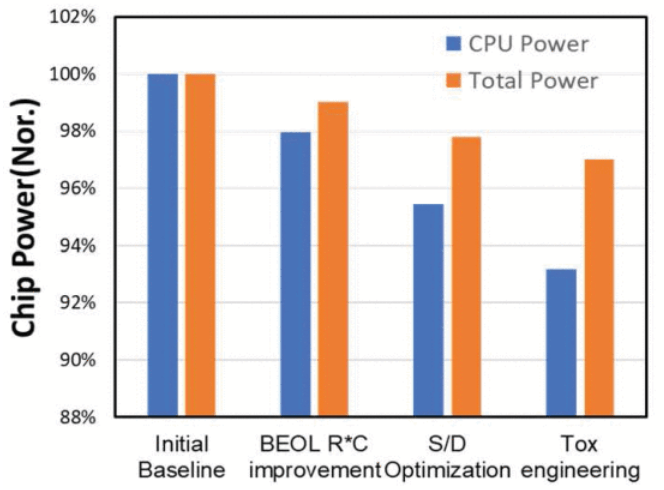
Fig. 1: FEOL source/drain and gate oxide thickness optimization as well as interconnect RC improvements reduced device power consumption. Source: Qualcomm/IEEE IEDM
Getting a working chip out the door was a challenge. Aggressive size scaling of fin pitch, gate pitch, and metal pitch, as well as SRAM cell area, initially resulted in multiple process hot spots, according to the team. Mitigating the top systematic defects required contact, gate, and epitaxy co-optimization. Metal-1 to Metal-2 voids were addressed with OPC tuning and tight in-line process control. “Yield loss at low-voltage operation mode was reduced by 5X as compared to initial baseline, with testing and process integration optimizations on several modules including spacer/liner optimization, device Vt centering, new OPC mask, and replacement metal gate (RMG) cleaning,” they wrote in a paper presented at the recent IEDM conference. “Design and DFT modifications effectively reduced resistive failures for tighter Vmin distribution at low voltage.”
Dynamic voltage screening and very low voltage memory repair helped to remove outliers, increasing the margin to specification. The 5nm CPU achieved >10% better performance at the same power as the 7nm device, or 15% lower power at the same speed.
To support all-day battery life, total power was addressed through epilayer front-end source and drain tuning and gate oxide engineering. Within-wafer process loading improvements were performed at several process steps for the fin, polysilicon, source/drain and RMG modules (see figure 1). Middle-of-line and BEOL interconnects were optimized for lower RC by minimizing the impact of barrier layers, creating vias with uniform height and optimizing etch stops (see figure 2). The team added that second-year process enhancements provided power-performance benefits, including 5% speed improvement with the same design from further gate optimization, FEOL cap layer reduction, and MOL resistance reduction.
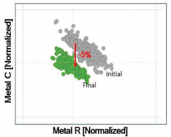
Fig. 2: Tuning of barrier layer, via height, and etch stop layer reduced the RC constant by 5%. Source: Qualcomm/IEEE IEDM
Extending 3D NAND
3D NAND is now ubiquitous in PCs, mobile devices, and data centers, and it is quickly making its way into automotive and neural networking applications. Charge-trapping flash (CTF) in 3D configurations scales inexpensively by stacking wordlines, using multitudes of deposition, etching, filling, and annealing steps, and fewer lithography patterning steps (relative to logic). Bit density follows an aggressive 30% increase per year.
To significantly reduce die size, all leading NAND manufacturers began fabricating the CMOS peripheral circuits underneath the memory array. Samsung was the first to bring to market its cell over peripheral (COP) V-NAND around 2010. But the real engine behind increasing bit density is repeated layer stacks — using multiple deposition steps, high-aspect-ratio etch, and high-AR fill capability to accelerate the number of storage wordlines in the array (tiers). These tiers stand at 200+ for Samsung, Micron and Hynix, all of which have roadmaps for 1,000 layers by 2030.
Russ Meyer and colleagues at Micron discussed several knobs to further increase NAND bit density and performance including alternative block architecture, new cell films, and pitch scaling options. “3D NAND has continued to deliver and even accelerate the NAND scaling trend that the data industry demands, in part due to its larger gate area and improved electrostatics of the gate-all-around (GAA) architecture.” Continuation on this path will lead to 1,000 tiers in the next 5 to 6 years, and die thickness nearing 100µm, unacceptable for many applications.”
By adding 50% more WL layers (the wordlines act as the gate and surround the pillar channels), the structure can suffer from wobbling and instability. That, in turn, can lead to failures like WL leakage, cell formation issues, and bit-line contact misalignment. One strategy Micron is exploring is a change from a 9-pillar block to a 19-pillar block that has about 2X the structure width and is compatible with the current block architecture of 4-pillar select gates (sub-blocks) used by several manufacturers (see figure 1). The change enables 9% cell area reduction.
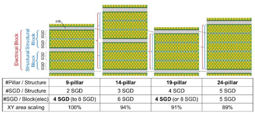

Fig. 3: NAND array scaling associated with changing from a traditional 9-pillar structure (pillar rows/block) to 19-pillar, for instance, enables a 9% smaller block, which is compatible with 4-pillar sub-blocks. Source: Micron/IEEE IEDM
X-Y scaling, which encountered its limit with planar NAND, is being approached with 3D NAND. Other concerns include device degradation caused by cell-cell coupling (i.e., noise). One step, WL gate replacement, becomes more challenging with the 19 pillar wider block architecture. The aspect ratio for the sacrificial tier removal and WL metal fill is larger, causing poorer metal step coverage (and higher WL resistance), as well as halogen contamination in voids and seams. The group found that a thinner alternative barrier metal can better protect from halogen impurities, enabling lower resistivity of the bulk tungsten fill.
Array height increases also can be mitigated by cell pitch scaling, making the pitch between pillars. The etching aspect ratio does increase moderately with the tighter pitch, but the greater issue is the impact to read performance at reduced channel width. Novel integration schemes are needed.
The Micron group further indicated that future NAND could incorporate more than 4 bits per cell. However, more bits per cell causes steeper loss in the number of electrons per state relative to the gain in volume bit density. “It is more reasonable to scale the dimension of the cell device first (e.g., preferably pillar pitch XY scaling) to the limits of the process capability. Innovative block architecture and WL driver schemes are key for 3D NAND performance scalability for coming nodes,” they concluded.
As companies continue 3D NAND scaling, they are observing a relationship between stress distribution in 3D flash structures and electrical performance. Made up of tunneling oxide, charge-trapping nitride, tungsten and polysilicon channels, both lattice mismatch and thermal mismatch between different materials cause mechanical stress. Thermal annealing does cause some relaxation, but the net mechanical stress in these increasingly confined 3D NAND structure can still have a great impact on electrical performance, according Pohang University of Science and Technology and Samsung (see figure 3). [3]
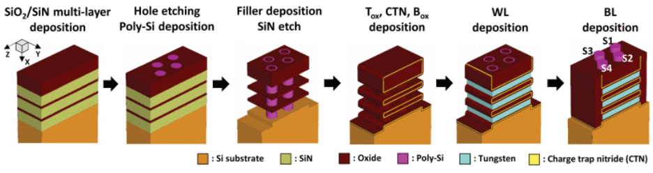

Fig. 4: Multiple deposition, high aspect ratio etching, and fill steps create the charge-trapping NAND sandwich. Source: IEEE J. EDS [2]
Interestingly, simulations determined that lowering the deposition temperature of tungsten (from 400°C) had the most pronounced impact on stress, shifting the conduction and the valence bands of the polysilicon channel, boosting the on-current and, therefore, read and write speeds.
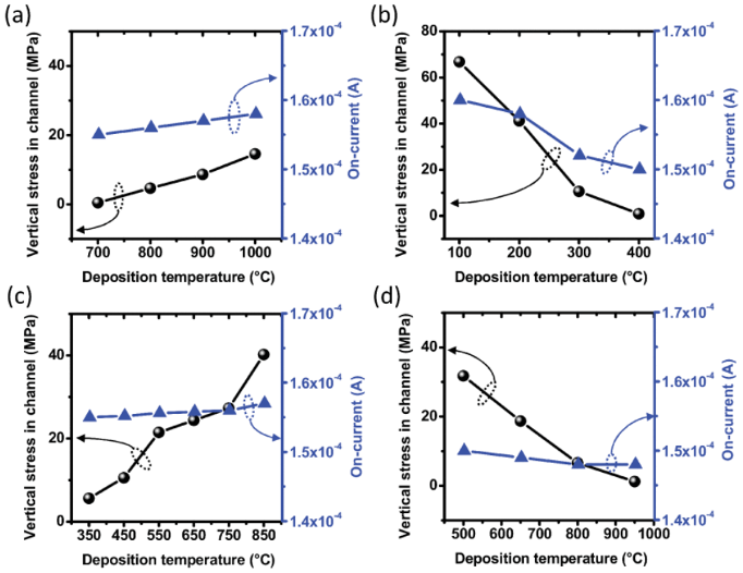

Fig. 5: Vertical stress vs. change in on-current for polysilicon (a), tungsten (b), tunning oxide (c), and charge trap nitride (d). Source: IEEE J. EDS [3]
The researchers highlighted that the charge trap nitride and tungsten have higher CTEs (coefficients of thermal expansion) relative to the tunnel oxide (SiO2) and polysilicon. Increasing tungsten and nitride deposition temperature effectively induce compressive stress and decrease on-current without impacting the memory process window and threshold voltage of devices. Further simulation showed that by lower the tungsten deposition temperature had the greatest influence on performance.
With all these narrow, high-aspect-ratio holes, it is no surprise that gap filling is a critical need in 3D NAND — especially since deposition temperatures are in the 300°C to 900°C range. One example of a recent development is a spin-on carbon material from Brewer Science, which has been used to fill 0.5 x 10µm trenches with no evidence of film voiding, cracking, or delamination after heat treating at 550°C for 60 minutes. [3] The thermally stable spin-on carbon exhibits minimal shrinkage and mass loss. Following spin coating, it uses soft bake and hot plate curing, followed by furnace nitridation if needed.
Extending DRAM for AI, automotive
Rapidly growing applications in machine learning and AI, as well as automotive, demand increased bandwidth for DRAMs. These peripheral circuits perform different functions (i.e., for row/columns decoders, sense amplifiers, I/O data buffers), and therefore require optimized transistors with low gate leakage, off current, and high breakdown voltage, as well as DRAM process compatibility. That’s true even for polysilicon/oxide planar FETs. In finFET transistors using high-k metal gates, flows must be optimized to withstand long, high-temperature anneals (4 hr at 550°C) and maintain electrical characteristics.


Fig. 6: Gate-first diffusion and gate replacement (left) result in higher threshold voltage and fewer metal gate options for work-function tuning relative to the gate-last high-k, replacement metal gate process (right). Source: imec/IEEE IEDM
Elena Capogreco and colleagues at imec recently demonstrated a 14nm high-k/metal gate replacement gate approach that can achieve sub-0.2V nMOS threshold voltage while enduring long duration anneals. [4] “In addition to the reduced thermal budget, another advantage of using RMG flow as compared to the gate-first diffusion and gate replacement scheme (see figure 2), is the increased freedom of WFM (workfunction metal) engineering between nMOS and pMOS.”
The researchers explained that while gate-first HKMG in low-cost CMOS finFETs for peripheral DRAM circuits already has been achieved, the threshold voltage is relatively high as a result of Fermi-level pinning (especially on pMOS devices) caused by high-temperature annealing. The new, thermally stable gate stack includes a 1nm interface oxide, 1.9nm hafnium oxide, 2nm TiN, 5nm TiAl, 3nm TiN and tungsten CVD and CMP.
Target gate length is 30nm. Some of the processing lessons learned include the need to cap the tungsten with silicon nitride to suppress gate oxide degradation from annealing. Nitride capping after CMP further encapsulates the metal. Effective workfunction for nMOS was optimized by annealing the hafnium oxide in nitrogen, followed by a sacrificial silicon cap anneal to improve its thermal stability. For lanthanum dipole gate stacks, 6-angstrom LaO was deposited by ALD and capped with 2nm TiN and 5nm sacrificial a-Si. Drive-in anneal and wet removal of a-Si leaves TiN under the TiAl and W. The capped gate stack endured 4 hours of 550° to 600°C annealing. The final effective workfunction was 4.4eV, with reduced gate leakage and effective oxide thickness of 14 angstroms. Performance was demonstrated with ring oscillators and SRAM. Next steps for imec will involve further pFET optimization for these peripheral DRAM circuits.
Conclusion
3D NAND scaling has been a boon to mobile device functionality and chip makers are continuing to stack wordline layers for increased performance and bit density. Eventually, NAND devices may require alternative materials, new configurations, or even greater than four bits per cell.
In the meantime, 5G SoCs continue to deliver high performance and long battery life to mobile phone users, and there does not seem to be any immediate limitation. However, none of this is going to be easy. Both transistor and interconnect optimizations are key to scaling to 5nm processes and beyond, and peripheral DRAM circuits optimized for low power and low leakage are more sensitive to high thermal budget processes. The good news is that workfunction tuning and replacement high-k metal gate appear to be enablers.
References
1. Y. Suh et al., “High Performance 5G mobile SoC Design-Technology Co-Optimization for PPA and Manufacturability with 5nm EUV FinFET technology,” 2022 International Electron Devices Meeting (IEDM), San Francisco, CA, USA, 2022, pp. 27.4.1-27.4.4, doi: 10.1109/IEDM45625.2022.10019545.
2. E. -K. Jang, I. -J. Kim, C. A. Lee, C. Yoon and J. -S. Lee, “Analysis of Residual Stresses Induced in the Confined 3D NAND Flash Memory Structure for Process Optimization,” in IEEE Journal of the Electron Devices Society, vol. 10, pp. 104-108, 2022, doi: 10.1109/JEDS.2022.3140774.
3. C. Jones, et. al., “High-Temperature-Stable, Spin-On Carbon Materials for High-Aspect-Ratio Gap-Fill Applications,” 2021 32nd Annual SEMI Advanced Semiconductor Manufacturing Conference (ASMC), Milpitas, CA, USA, 2021, pp. 1-4, doi: 10.1109/ASMC51741.2021.9435713.
4. E. Capogreco et al., “FinFETs with Thermally Stable RMG Gate Stack for Future DRAM Peripheral Circuits,” 2022 International Electron Devices Meeting (IEDM), San Francisco, CA, USA, 2022, pp. 26.2.1-26.2.4, doi: 10.1109/IEDM45625.2022.10019422.
Related Story
Is There A Limit To The Number Of Layers In NAND?
Challenges continue to mount, but most of them appear surmountable with enough investment
- SEO Powered Content & PR Distribution. Get Amplified Today.
- Platoblockchain. Web3 Metaverse Intelligence. Knowledge Amplified. Access Here.
- Source: https://semiengineering.com/process-innovations-enabling-next-gen-socs-and-memories/

