Creating real 3D designs is proving to be much more complex and difficult than 2.5D, requiring significant innovation in both technology and tools.
While there has been much discussion about 3D designs, there are multiple interpretations about what 3D entails. This is more than just semantics, however, because each packaging option requires different design approaches and technologies. And as chips push into the realm of real 3D-ICs, stacking logic or memory on top of logic, they become much more challenging to design, manufacture, and ultimately yield and test.
“In the beginning, the foundries starting to offer multi-die packaging, and they started using this term 3D-IC,” says John Park, product management group director in the Custom IC & PCB Group at Cadence. “But It referred to more than just silicon stacking and interposers. It also included high-density RDL fanouts. It was a term used to group a lot of multi-die, mostly foundry-based packaging technology.”
There have been several attempts to sort out this terminology. “We are aligning with imec, which split 3D into four segments,” says Thomas Uhrmann, director of business development at EV Group. “True 3D is wafers stacked on top of each other in a highly integrated way. The second group would be 3D system-on-chip (SoC) integration, where you might have a backside power distribution layer, or a wafer-to-wafer stack of memory. The third group includes 2.5D and silicon interposers. And the final one is 3D system-in-package (SiP), where contact pitches are about 700 microns, including fan-out wafer-level packaging. The differentiation is interesting, because they are defining the differentiation over contact pitch or integration density.”
This provides a physical differentiation, but differences also can be looked at in other terms. “The interesting kinds of 3D are either logic-on-logic, or significant memory-on-logic,” says Rob Aitken, a Synopsys fellow. “Both of those are starting points, but then you can start stacking other random things. I would say that HBM are 3D stacks, but they’re a very specific 3D stack.”
The flows for each of these packaging approaches is different. “2.5D and 3D have been used for several years to be able to support things like sensor applications,” says Tony Mastroianni, advanced packaging solutions director at Siemens EDA. “But they don’t use an automated place-and-route flow, and that’s why I like to use the term ‘true 3D.’ Stacked die technology today relies on people doing planning manually. You are designing each chip so they butt together, but the tools are not doing that. The partitioning and the detailed pin planning are manual processes.”
True 3D requires a rethinking of the entire flow. “For the efficient implementation of an SoC as a 2.5D system, such as avoiding yield problems or to realize bigger systems with more transistors, existing architectures can be used,” says Andy Heinig, head of department for efficient electronics at Fraunhofer IIS’ Engineering of Adaptive Systems Division. “Only a chip-to-chip interface must be implemented. But the advantages of a real 3D integration can only be exploited if new concepts and architectures are used.”
Why go to 3D
One of the biggest benefits for 3D is reduced distances. “You can make an argument that there’s a square-root-of-two effect,” says Synopsys’ Aitken. “For all of the distances in this stacked object, they become 0.7 of what they would have been in the 2D variant. As a result, the power they consume on the wiring part is now 0.7-ish of what it was before because the capacitance is reduced.”
The impact could be larger than that. “A lot of heat is generated in the transport of signals,” says EV Group’s Uhrmann. “For CMOS, you charge and discharge something in order to store and then to pass on the information. Shrinking and stacking the dies will enable you to make it smaller, so information can be passed in the third dimension. But you probably only have a buffer between them in 3D, rather than a large PHY and communication protocol.”
Two advantages come from size — yield and footprint. “Assuming a similar amount of logic distributed across multiple dies, the yield of your smaller objects will be higher than the yield of one bigger object,” says Aitken. “Therefore, you can reduce some level of cost. Of course, you are increasing other costs, but those will come down over time.”
From a 2D footprint perspective, stacking die can significantly reduce area. “By stacking, I can get three times the amount of logic in the same area,” says Siemens’ Mastroianni. “You end up with a much smaller footprint with a lot more logic. So you can fit a lot more horsepower in that area, and if you have area restrictions it might lower system costs.”
Heterogeneity could be another benefit. “Heterogeneous technology architectures are ripe for 3D integration,” says Maurice Steinman, vice president of engineering for Lightelligence. “Consider mixed technology assemblies, such as a photonic IC with its companion electronic IC. For some of these integrations, there is simply no other way to provide the many thousands of required die-to-die interconnections without substantial power or performance sacrifices.”
Mixing technologies is still mainly uncharted territory. “If your design doesn’t fit in a reticle size, then to be able to build more gates, you need to go to the true 3D, and that probably will stay in the same technology,” says Mastroianni. “But there’s certainly instances where you might want to mix and match. Maybe you have a compute engine that really you want in the bleeding edge technology, but the rest of the stuff has a lot of control that you could do in a less aggressive process node.”
That turns into an integration challenge. “We have recently seen that pure memory on logic configuration works for certain types of customers who are trying to solve the on-chip memory wall problem,” says Vinay Patwardhan, product management group director in the Digital & Signoff Group at Cadence. “But a lot of customers want to have logic on both tiers. For example, even if you just have memory on the top die, then the memory BiST logic or the test logic that goes with the memory needs to be on that die, as well. There is a need for some logic on that top die.”
Physical hierarchy
The integration of chips into a 3D stack, and the packaging of that stack, involve a number of technologies, as shown in figure 1.
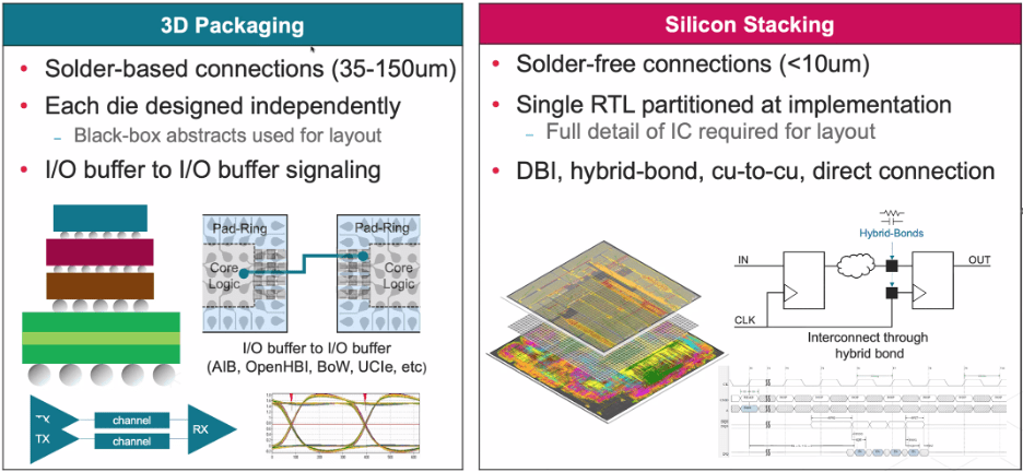
Fig. 1: 3D packaging versus silicon stacking. Source: Cadence
Physical dimensions matter. “For the ultimate 3D integration, you’re talking about 14nm pitch, basically where transistors are today,” says Uhrmann. “If you’re talking about chiplets, which are functional IP blocks, you’re in the range of somewhere like micron pitch. There is close to an order of magnitude between transistors stacking and chiplet integration. When you’re forming a 3D package, using a 3D chiplet, using a highly integrated die with a micron pitch, you cannot connect the micron pitch to the outside world. You still need to have the packaging technologies in order to get the routing coarser and coarser, so you eventually get them to 400-plus microns on the board level.”
The pitch defines the integration process. “There are some big differences in packaging when we’re packaging multiple dies or multiple chiplets,” says Cadence’s Park. “Chiplets typically use what are referred to as solder-based connections. They’re connected with micro bumps and C4s, and we work with connections that are usually around 45 microns and larger to connect those. This also creates a packaging hierarchy, because oftentimes we work with black box, abstract representations of each of the die or chiplets, and it’s a package designer that’s responsible for connecting them all up correctly.”
That usually requires different tooling for each. “This is a multi-scale problem, which also means a multi-physics issue,” says Marc Swinnen, director of product marketing at Ansys. “When you go from nanometers on a chip through millimeters on a package through centimeters on a 3D-IC interposer, that is six orders of magnitude you’re crossing there. Traditionally, those have been handled by three different sets of tools. Now for 3D-IC, these all need to be consolidated into a single one.”
Team-splitting causes problems, too. “Most companies have design groups for ASIC design, and separate internal package design groups,” adds Park. “Silicon stacking and 3D has blurred the line between what a package engineer is responsible for versus the die design team. We see, more than ever, the two teams in a single room planning the project from the early stages. There are many requirements for co-design between the domains of package and die.”
In some companies, the interposer also was seen as being a PCB within the package, and handled by yet another team. “3D chips are going to be doing some very advanced type function, but you’re not necessarily going to be able to build your whole system and package by stacking dies,” says Mastroianni. “You will combine that with other dies on an interposer. Maybe there will be a standard processor out there, or maybe multiple 3D-ICs that you’re integrating together on an interposer. I don’t think 3D is going to displace to 2.5D. They will be complementary. Some applications will be true 3D, but there will be an ecosystem eventually of some chiplets that you’re going to be able to mix and match, and do that in a 2.5D package.”
Wherever hierarchy exists, it is possible for things to be separated, so long as tools exist to cover the boundaries. “We have to represent things in a hierarchy form because you’re not designing a single monolithic chip anymore,” says Park. “You’re designing a system, and so there are new things that come into play like system LVS (layout versus schematic). Are the hybrid bonds all aligned? Are the connections going as you expect them, from the top die through the bottom die? There’s a hierarchy just in the fact that you have a hierarchy representing die and you have a hierarchy representing the system-level design. Design, by nature, is hierarchical because it’s a system-level design that has embedded in it die-level designs.”
Logical hierarchy
Hierarchy is a must in any complex design, but 3D adds an interesting twist to it. “When you’re doing traditional place-and-route for large designs, you’re using a hierarchical design approach,” says Mastroianni. “You break the design up into blocks, and those blocks go through place-and-route, and then you do your top-level integration. For 3D, we can essentially use the same process, but we’re adding another level of hierarchy. Consider a 9 billion-gate design, where we break this into three chips, each with 3 billion gates. Essentially, you just need to specify which blocks will go on chip 1, which blocks will go on chip 2, and those that will be the blocks in chip 3. At least in the near term, tools will not be able to automatically figure out which logic to put where, and do a true 3D global place-and-route at that level. There are some longer-term DARPA proposals that are looking to do that, but even those proposals are not in the first phase.”
Some new tools would be required to verify the chip-to-chip connectivity. “We would typically be using a standard flop-to-flop connection,” says Park. “So we need STA tools, timing-driven routing, timing-driven placement, and instead of a buffer separating the devices, it’s just a hybrid bond. It’s just a small parasitic value that comes into play. For this, we can’t work at the abstract level, like traditional packaging, where these are treated as black boxes. We have to represent each of the chips or chiplets at the full detail level — full transistor level if its analog design, standard cell macro level if it’s a digital design — because we have to be able to model everything. Instead of modeling everything from a 2D perspective, it has to be done with this new vertical direction integration.”
That may require compromises. “You can either have a true 3D signoff of the logic stacked object, or you can just say, I’m only going to run paths that are two inverters long between the die,” says Aitken. “Then whatever corners they are, they will just line up and I don’t have to worry about it.”
There is widespread agreement that doing it flat is not an option. “It would be a significant challenge for any of the EDA tools, just because of the amount of data,” says Cadence’s Patwardhan. “Some effective abstraction techniques are needed, and hierarchy definition is the first thing that is popular and is working. We have figured out, using design hierarchy, as well as partitioning a design, how to make analysis run on a partitioned design. What assumptions can be made and still have accuracy as good as signoff. It will happen, as it happened in the 2D SoC. Smaller designs will first establish a full flat run and the level of accuracy needed, (measured versus modeled). As we go forward, as larger chips get done in a silicon stack format, there will be some correlation that EDA, OSATs, and foundries will have to prove between a hierarchical method and the flat method, to be within a certain margin. And if that’s available, then you can comfortably say that your full flat run is going to look the same. It’s a very important methodology in 3D-IC design, and it won’t be all flat.”
This becomes a lot more difficult when full 3D place-and-route becomes possible. “The safe answer today is to say, ‘Let’s not divide blocks. Let’s just keep each block on one die and we’ll talk to them across the die boundary.’ Doing that, you still have a 3D placement partitioning problem that you have to solve, but your signoff problem is simpler because at least your block signoff is confined to the 2D space,” says Aitken. “Academic works suggest that moving blocks and interspersing them across a boundary can gain you extra benefit. But for the most part, those papers have ignored things like clock synchronization, die matching, and other problems that will show up when you try to do something like that. If you keep individual blocks on a single die, you still have a whole lot of problems to solve, but it’s a smaller number of problems than if you allow the blocks to migrate across the die.”
- SEO Powered Content & PR Distribution. Get Amplified Today.
- Platoblockchain. Web3 Metaverse Intelligence. Knowledge Amplified. Access Here.
- Source: https://semiengineering.com/true-3d-is-much-tougher-than-2-5d/

