The “1.xnm” node on most roadmaps to indicate a 16-18 nm metal line pitch [1]. The center-to-center spacing may be expected to be as low as 22-26 nm (sqrt(2) times line pitch). The EXE series of EUV (13.5 nm wavelength) lithography systems from ASML feature a 0.55 “High” NA (numerical aperture), targeted toward enabling these dimensions. The only justification for this projected resolution is that it exceeds about one-third wavelength/NA. Some reality checks are in order to confirm the realism of this expectation.
1. Plane of Incidence Rotation Across Slit
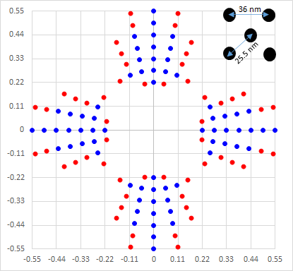
The plane of incidence is known to rotate across the EUV exposure arc-shaped slit [2]. Consequently, the optimized illumination distribution for a given pattern actually rotates across slit, potentially giving unoptimized results at slit positions toward the edge compared to the center.

Figure 1. The optimized source (red) for a 25.5 nm center-to-center array needs to be trimmed down (blue) to be safe against rotation across slit.
As shown in Figure 1, trimming the optimized source allows it to be safe against slit rotation effects, but this also reduces pupil fill, i.e., the range of illumination angles divided by full range of possible angles. Below 20% pupil fill, the EUV illumination system itself begins absorbing the EUV energy, which is not desired not only due to system wear, but also due to reduced throughput [3].
2. Low NILS
The 1.x nm node may be expected to feature 22-25 nm center-to-center vias with sizes <10 nm. Such small vias (already less than the Rayleigh resolution) at relatively wide spacings will have a low normalized image log-slope (NILS) without a slower exposure [4]. Phase-shift masks need to be designed for EUV use, but this is still under development.
3. Polarization
As line pitches shrink to 18 nm and below, polarization begins to become important since the angle between interfering waves is larger [5,6]. Moreover, the multilayer in an EUV system preferentially reflects in the TE polarization, i.e., perpendicular to the plane of reflection; this is (mostly) perpendicular to the scan direction) [6]. This will degrade the NILS of lines which are aligned with the scan direction, i.e., horizontal lines.
4. Thinner Resist
Resist thickness is expected to be reduced to below 30 nm in order to be used with High-NA EUV systems. This is due to the reduced depth of focus [7]. Even with improved depth of focus, however, aspect ratio of smaller features is another likely limiting factor. A 10 nm wide feature with a 20 nm resist thickness already has an aspect ratio of 2:1. A reduced resist thickness must be compensated by an inversely proportional higher absorption coefficient in order to preserve absorbed photon density for a given dose.
5. Electron Blur and Stochastics
Finally, focusing EUV to a smaller spot would be no use in the presence of over 3 nm blur [8]. However, the randomness of secondary electrons [9,10] prevents blur from being a fixed number, ultimately leading to the possibility of stochastic defects [11].
All the above factors should serve as reminders that advancing lithography is no longer a simple matter of reducing wavelength and/or increasing numerical aperture.
References
[1] International Roadmap for Devices and Systems (Lithography), 2022 edition.
[2] M. Antoni et al., “Illumination optics design for EUV lithography,” Proc. SPIE 4146, 25 (2000).
[3] F. Chen, High NA EUV Design Limitations for sub-2nm Nodes, https://www.youtube.com/watch?v=IgYJfLyDYos
[4] F. Chen, Phase-Shifting Masks for NILS Improvement – A Handicap for EUV?, https://www.linkedin.com/pulse/phase-shifting-masks-nils-improvement-handicap-euv-frederick-chen
[5] H. Levinson, “High-NA EUV lithography: current status and outlook for the future,” Jpn. J. Appl. Phys. 61 SD0803 (2022).
[6] F. Chen, The Growing Significance of Polarization in EUV Lithography, https://www.linkedin.com/pulse/growing-significance-polarization-euv-lithography-frederick-chen; F. Chen, Polarization by Reflection in EUV Lithography Systems, https://www.youtube.com/watch?v=agMx-nuL_Qg
[7] B. J. Lin, “The k3 coefficient in nonparaxial l/NA scaling equations for resolution, depth of focus, and immersion lithography” J. Micro/Nanolith. MEMS MOEMS 1(1) 7–12 (April 2002).
[8] T. Allenet et al., “Image blur investigation using EUV-Interference Lithography,” Proc. SPIE 11517, 115170J (2020), https://www.dora.lib4ri.ch/psi/islandora/object/psi%3A38930/datastream/PDF/Allenet-2020-Image_blur_investigation_using_EUV-interference_lithography-%28published_version%29.pdf
[9] Q. Gibaru et al., Appl. Surf. Sci. 570, 151154 (2021), https://hal.science/hal-03346074/file/DPHY21090.1630489396_postprint.pdf
[10] H. Fukuda, J. Micro/Nanolith. MEMS MOEMS 18, 013503 (2019).
[11] F. Chen, Secondary Electron Blur Randomness as the Origin of EUV Stochastic Defects, https://www.linkedin.com/pulse/secondary-electron-blur-randomness-origin-euv-stochastic-chen
Also Read:
Can Attenuated Phase-Shift Masks Work For EUV?
Lithography Resolution Limits: The Point Spread Function
Resolution vs. Die Size Tradeoff Due to EUV Pupil Rotation
Share this post via:
- SEO Powered Content & PR Distribution. Get Amplified Today.
- PlatoAiStream. Web3 Data Intelligence. Knowledge Amplified. Access Here.
- Minting the Future w Adryenn Ashley. Access Here.
- Source: https://semiwiki.com/lithography/327889-reality-checks-for-high-na-euv-for-1-x-nm-nodes/


