The promise of scalability and efficiency is accelerating the migration of electronic design automation (EDA) to the cloud. Unlimited on-demand compute resources fundamentally change the chip design paradigm, where tools and workloads are no longer constrained by localized hardware.
This is easier said than done, however. Optimizing existing tools and infrastructure, creating a new generation of EDA applications that run natively on the cloud, and integrating advanced AI capabilities across the development stack are non-trivial for both EDA vendors and chip companies. Chipmakers have developed flows and customized tools for their specific needs. How much of that customization will carry over to the cloud may determine which tools and workloads to keep on-premises.
These considerations will require a thorough evaluation of capabilities, requirements, and silicon design strategies. But as chip designs become increasingly heterogeneous and complex, and as partitioning becomes more workload specific, there is a growing recognition that at least some aspects of design will require cloud resources to both accelerate time-to-results and remain innovative and agile in a highly competitive market.
Managing EDA in the cloud
Most large chip companies have adopted a hybrid model, shifting select EDA tools and workloads to clouds managed by in-house IT teams. Many silicon startups, meanwhile, have never invested in pricey on-premise tools, opting instead for end-to-end cloud-based EDA. For these companies, every stage of the chip design process — design, verification, debug, and test — happens entirely on a vendor-managed cloud.
“There are many, many customers who are born in the cloud,” said Vikram Bhatia, head of cloud product management and GTM strategy at Synopsys. “They don’t have on-premises hardware resources set up to do any type of EDA. They just do everything in the cloud. And then there are customers who have very large on-premises data centers, some bigger than cloud provider data centers. They’re also using cloud, but the needs are slightly different.”
These large customers may have specific workloads or projects that can benefit from cloud instances managed by EDA vendors. “They can quickly get up and running in a few weeks, with a few hours of setup time and just do what they need to do,” Bhatia said. “They can run a few workloads quickly.”
Nevertheless, the percentage of large chip companies developing a significant portion of their designs in the cloud remains relatively small. Major silicon vendors dedicate extensive budgets to optimize their own cloud EDA operations. In contrast, smaller silicon startups, and even medium-sized companies may prefer vendor-managed turnkey cloud instances that dynamically optimize tools and infrastructure to accommodate specific workloads.
“Many companies are starting fresh, so they don’t have the legacy infrastructure data centers,” said Mahesh Turaga, vice president of business development for cloud at Cadence. “Medium-sized companies do have some data center capacity, but can’t scale quickly enough. So these are all the ideal situations for them to really say, ‘Can you give us this turnkey environment to do this in the cloud?’ Larger companies already have a lot of huge data center investment, but then they are bringing in cloud into their own environments to tackle the peak usage needs and tend to do this in a customer managed cloud.”
Any company with scale has had years and years of investment in their own data centers, so larger customers aren’t necessarily looking for software that’s managed by the EDA vendor. “If you think of it like a more traditional SaaS, where you only have a login and you’re able to access the functionality through your browser, that’s not attractive to larger companies doing multiple projects with hundreds and hundreds of engineers and global footprints,” observed Craig Johnson, vice president of cloud solutions at Siemens EDA. “Those customers are going to the cloud on their own.”
Managed cloud offerings are a good choice for smaller companies that lack large design teams, as well as on-premises infrastructure. “If you’re a startup on the silicon side, you’ve got your architects, you’ve got some of your verification experts engaged, but you don’t always have your back-end people in place yet,” Johnson said. “Some companies will outsource the back end to an ASIC provider or someone who will do the layout for them, but project needs change over the course of a year or two. That’s when flexible all-in-one packages can make a lot of sense.”
Optimized versus cloud-native EDA tools
EDA vendors continuously optimize their tools in the cloud to streamline end-to-end chip design workflows. Concurrently, they work closely with customers to develop new cloud-native EDA tools. Rather than a traditional lift and shift (or port and optimize), these tools offer new flexible licensing models and feature a specialized user interface (UI) to accommodate cloud-native workloads, libraries, and file structures.
One such example is DSim Cloud, which Metrics Design Automation offers as a Kubernetes-based SaaS. “You log in, you start using it,” said Joe Costello, executive chairman at Metrics. “I don’t have to worry at all about managing my machines and data — where it’s going to be and how it’s going to be handled or stored. It doesn’t matter if I use a thousand computers for one second, or one computer for a thousand seconds. We charge by the minute, not a license. That’s what fundamentally makes our approach completely different than what people have been doing in EDA to this point.”
Also, DSim Cloud’s UI was built from the bottom up, rather than ported over from legacy on-premises tools. This cloud-native approach eliminates frustrating user experiences that some have compared to running Informix-4GL or FoxPro on modern versions of Windows.
“When I want to see my results, I don’t have to download a huge waveform file to my computer, take all that time and energy to parse through it and make some changes,” Costello noted. “I can do all the analysis and debug in the cloud, IDE style, which is simpler, cleaner, and easier. After all, a hardware description language is software. So, that kind of environment makes a lot more sense.”
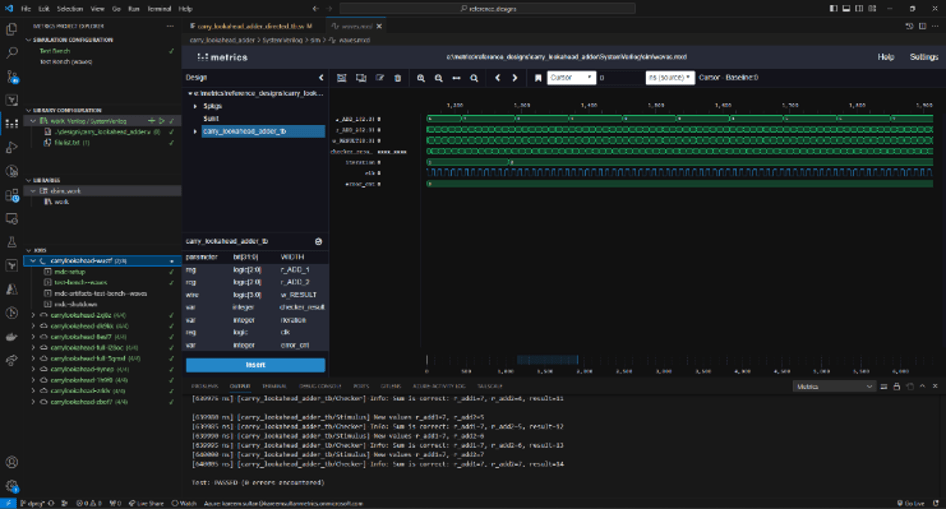
Fig. 1: DSim Cloud interface display, showing real-time waveform simulation results for a cloud-submitted job. Source: Metrics
Developing cloud-native EDA tools remains an industry challenge, however, due to traditional licensing models and the sweeping infrastructure changes it requires. “You have to rewrite your core cloud infrastructure. It has to be Kubernetes-based,” Costello added. “You have to rewrite your user interface to make it cloud-oriented. That’s hard work, but it’s not rocket science.”
Indeed, most EDA applications traditionally were written in lower-level languages such as C or C++ and optimized for on-premises performance. “The algorithms themselves are compute-intensive and get into very fine control of what processes run in parallel, what is staged in sequence, and how much memory you allocate,” said Siemens’ Johnson. “All of that is very, very controlled at the application level, and if you start from scratch on the cloud, you have to redo all your algorithms and software and essentially double the size of your engineering team.”
Most cloud-native applications are likely to emerge in areas where they aren’t simply repeating functionality. The Siemens EDA portfolio, for example, includes a number of cloud-native applications, including PartQuest, which connects PCB development teams to the electronic component ecosystem, and Connect for PADS Professional to streamline collaboration.

Fig. 2: Siemens’ PartQuest Explore interface, showcasing access to comprehensive simulation model libraries from industry. Source: Siemens EDA
“There are places where we have cloud-native right now on the system side with PCB, because of the collaborative nature of those design ecosystems,” Johnson said. “There’s years and years of work ahead for cloud-native applications, and ultimately our customers will be what determines the pace of adoption. All the while, we’re optimizing our tools on the cloud for parallelism, default tolerance, and memory footprint.”
All of the big EDA vendors have taken steps to create cloud-native EDA tools. “Tools that will drive this new generation of EDA are those that require collaboration in the cloud, between design teams, foundry partners, and chip designers with the single source of truth of the data residing in the cloud, accessible from anywhere, and on any device,” said Cadence’s Turaga. “PCB design tools in the Allegro and OrCAD families are perfect examples. We also have many of our tools architected for cloud, with hybrid capabilities, where customers can access cloud-based compute with the click of a button. Xcelium Cloud, ADE Cloud, Clarity Cloud, and OrCAD X are perfect examples of such architectures that make it seamless for users to leverage the power of cloud.”
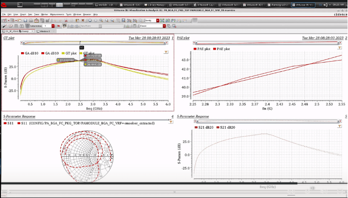
Fig. 3: Cadence’s Virtuoso EDA Suite, displaying various S-parameter responses and power-added efficiency (PAE) plots, can run on-premises or in the cloud. Source: Cadence
The role of AI EDA in the cloud
Many AI applications are considered cloud-native, creating an optimal environment for Synopsys.ai and its generative AI Co-Pilot. “Semiconductor customers designing chips are leveraging generative AI models hosted as a service in the cloud,” said Bhatia. “Obviously the tools that are being built are also leveraging this natively in the cloud. There are very few customers who are thinking of, or have even started their journey toward building their own models from scratch. Reinventing the wheel doesn’t make sense because it’s very, very expensive to build and train your own models.”
Synopsys ChipSpot, which helps semiconductor companies take advantage of lower-priced spot instances without interruption or arbitrary termination, is another example of an AI-based EDA solution that exists only in the cloud. Essentially, ChipSpot creates on-demand virtual machines (VMs) optimized for specific EDA tools and very high memory workloads. Prompted by predictive termination signals, ChipSpot automatically migrates live EDA workloads to and from its VM array.
“You are now taking cloud-native capabilities that are inherent to the infrastructure and applying it as a use case to the chip design model,” Bhatia said. “ChipSpot is fully cloud-native, and there are quite a few use cases — horizontal use cases are what I like to call them — infrastructure or horizontal solutions you can leverage that are cloud-native to the chip design use case.”
Harnessing AI and ML to scale EDA cloud workloads more efficiently and cost-effectively is another area of focus for many semiconductor companies. “The user may not know how many threads, parallel jobs, clusters, and memories are needed,” said Rajath Narasimha, principal product manager for cloud HPC at Keysight. “All these parameters should be automatically configured through a workspace analysis. You would say, ‘I want to simulate this within 20 minutes or two hours or 20 hours.’ Based on that, an algorithm should automatically set the requirements and send the jobs out.”
Narasimha said Keysight Design Cloud is a step in this direction, offering on-premises, hybrid, and turnkey cloud configurations. “For turnkey cloud customers, we provide an API to a company called Rescale, which accepts the job from a laptop or server environment and puts it in a queue. Based on the request you send them, they optimize it for cost, time, and location, as well as the type of computing and resources you require. Rescale and Keysight Design Cloud is really the cheapest way for startup companies to take advantage of EDA in the cloud. It is designed for companies that have two or three engineers and zero on-prem environments, except maybe a server which they can install things on. Computing resources are easy to access, on-demand, and scalable in the cloud — the best balance between scalability, performance, and customization.”
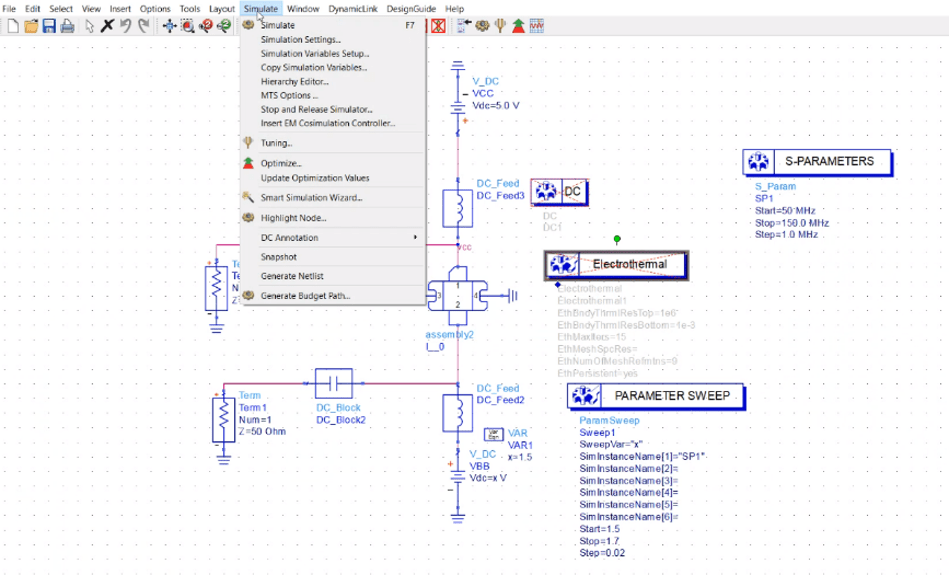
Fig. 4: Keysight’s Design Cloud interface with an API to Rescale, demonstrating an RF circuit simulation setup for S-parameter analysis and parameter sweeps, optimized for turnkey cloud EDA solutions. Source: Keysight
Verification, parallelism rule the EDA cloud
Although many EDA workloads are shifting to the cloud, verification is still the most popular for most chip companies due to its high-resource demands. “The places where there’s the highest interest in cloud is where there’s the highest volume of compute or the most difficult areas of compute,” Johnson said. “That tends to be logic verification on the front end, because of the endless numbers of simulations you run as you debug your design. Verification has a profile of compute that’s generally lots and lots of cores. The memory requirement isn’t that large, but you can use a tremendous number of machines in parallel.”
Different categories of verification tools are used throughout most of the silicon design lifecycle. For example, if a chip typically takes 18 months to develop, verification probably will run consistently for at least 15. “As you add more and more go to the next stage, you verify again and again and again,” Bhatia said. “Cloud speeds up everything. You can scale up very quickly. So let’s say for a particular step you had scheduled eight weeks to do your timing analysis. If you’re able to cut that down to five or six weeks, you’ve got two extra weeks of time. Now you can either release your chip faster, or do more verification and release a better-quality chip and still stay on schedule.”
While compute-intensive workloads were one of the original catalysts for the advent of EDA cloud, many chip companies are finding verification to be a gateway use case. “Generally, a lot of customers start with verification, but then we start to see they are moving entire projects to the cloud,” Turaga explained. “It’s not just verification anymore. It’s entire full flow and tape-out in the cloud. This is obviously the case with many small customers already fully in the cloud, but also for many of the larger ones who operate in hybrid environments, especially when a critical project comes up, just before a tape-out or whatever the situation is. They are basically executing full projects, full flows in the cloud.”
What remains on-premises
Although all EDA tools or workloads running on-premises ultimately can move to the cloud, some are likely to migrate slowly, while others may never complete the digital journey. “Some of the concerns we hear from some customers are around highly sensitive chip design data,” Turaga explained. “Some customers are still hesitant to put all of that in the cloud. There are also certain workflows that would give you much higher ROI in the cloud than on-premises, and that is always going to be the case. And some of those low-ROI workloads might stay on-premises.”
Bhatia agrees. “Traditionally, we’ve always thought of cloud as cheaper. But when you’re talking hundreds of thousands of cores of compute capacity needed to run a particular workload, and you have enough infrastructure on-prem for at that scale, cloud economies of scale are irrelevant because you have the same scale and on-prem is cheaper. Take the top 10 semiconductor companies and talk to any of them and they will tell you the same thing. The cloud is expensive, but they’re still going to it. I have no choice. I need to finish this job in one week instead of one month. So, I’ll pay what I need to pay.”
Bhatia also noted that IP concerns have resurfaced in recent months, as smaller startups designing complex, unique silicon fiercely compete with larger, more traditional chip companies. “It’s not so much security; it’s just IP protection. These startups are very stealthy,” he said. “They know that if anybody finds out what use cases they are targeting, it wouldn’t be very hard for a large organization with resources to try and copy. The need for security and secrecy is paramount, and that is something that will hold back — or is holding back — a lot of these organizations from putting certain types of projects on the cloud.”
But he added that while there may be various reasons for certain EDA tools and workloads to remain on premises, technology isn’t one of them. “The cloud is very, very advanced today. It’s been around for more than a decade and has evolved. The cloud is in gen six, gen seven of its original design, and you can do anything on it.”
- SEO Powered Content & PR Distribution. Get Amplified Today.
- PlatoData.Network Vertical Generative Ai. Empower Yourself. Access Here.
- PlatoAiStream. Web3 Intelligence. Knowledge Amplified. Access Here.
- PlatoESG. Carbon, CleanTech, Energy, Environment, Solar, Waste Management. Access Here.
- PlatoHealth. Biotech and Clinical Trials Intelligence. Access Here.
- Source: https://semiengineering.com/ic-tool-vendors-eye-cloud-native-future/

