On Wednesday, February 21st Intel held their first Foundry Direct Connect event. The event had both public and NDA sessions, and I was in both. In this article I will summarize what I learned (that is not covered by NDA) about Intel’s business, process, and wafer fab plans (my focus is process technology and wafer fabs).
Business
Key points in the keynote address from my perspective.
- Intel is going to organize the company as Product Co (not sure Product Co is the official name) and Intel Foundry Services (IFS) with Product Co interacting with IFS like a regular foundry customer. All the key systems will be separated and firewalled to ensure that foundry customer data is secure and not accessible by Product Co.
- Intel’s goal is for IFS to be the number two foundry in the world by 2030. There was a lot of discussion about IFS being the first system foundry, in addition to offering access to Intel’s wafer fab processes, IFS will offer Intel’s advanced packaging, IP, and system architecture expertise.
- It was interesting to see Arm’s CEO Rene Haas on stage with Intel’s CEO Pat Gelsinger. Arm was described as Intel’s most important business partner, and it was noted that 80% of parts run at TSMC have Arm cores. In my view this shows how seriously Intel is taking foundry, in the past it was unthinkable for Intel to run Arm IP.
- Approximately 3 months ago IFS disclosed they had orders with a lifetime value of $10 billion dollars, today that has grown to $15 billion dollars!
- Intel plans to release restated financials going back three years breaking out Product Co and IFS.
- Microsoft’s CEO Satya Nadella appeared remotely to announce that Microsoft is doing a design for Intel 18A.
Process Technology
- In an NDA session Ann Kelleher presented Intel’s process technology.
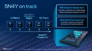
- Intel has been targeting five nodes in four years (as opposed to the roughly 5 years it took to complete 10nm). The planned nodes were i7, i4 Intel’s first EUV process, i3, 20A with RibbonFET (Gate All Around) and PowerVia (backside power), and 18A.
- i7 and i4 are in production with i4 being produced in Oregon and Ireland, and i3 is manufacturing ready. 20A and 18A are on track to be production ready this year, see figure 1.

Figure 1. Five Nodes in Four Years.
I can quibble with whether this is really five nodes, in my view i7, i3 and 18A are half nodes following i10, i4, and 20A, but it is still very impressive performance and shows that Intel is back on track for process development. Ann Kelleher deserves a lot of credit for getting Intel process development back on track.
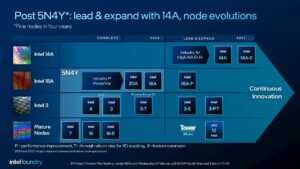
- Intel is also filling out their offering for foundry, i3 will now have i3-T (TSV), i3-E (enhanced), and i3-P (performance versions).
- I can’t discuss specifics, but Intel showed strong yield data for i7 down through 18A.
- 20A and 18A are due for manufacturing readiness this year and will be Intel’s first RibbonFET processes (Gate All Around stacked Horizontal Nanosheets) and PowerVia (backside power delivery. PowerVia will be the world’s first use of backside power delivery and based on public announcement I have seen from Samsung and TSMC, will be roughly two years ahead of both companies. PowerVia leaves signal routing on the front side of the wafer and moves power delivery to the backside allowing independent optimization of the two and reduces power droop and improves routing and performance.
- 18A appears to be generating a lot of interest and is progressing well with 0.9PDK released and several companies have taped out test devices. There will be an 18A-P performance version as well. It is my opinion that 18A will be the highest performance process available when it is released although TSMC will have higher transistor density processes.
- After 18A Intel is going to a two-year node cadence with 14A, 10A and NEXT planned. Figure 2 illustrates Intel’s process roadmap.

Figure 2. Process Roadmap.
- Further filling out Intel’s foundry offering they are developing a 12nm process with UMC and a 65nm process with Tower.
- The first High NA EUV tool is in Oregon with proof points expected in 2025 and production on 14A expected in 2026.
Design Enablement
Gary Patton presented Intel’s design enablement in an NDA session. Gary is a longtime IBM development executive and was also CTO at Global Foundries before joining Intel. In the past Intel’s nonstandard design flows have been a significant barrier to accessing Intel processes. Key parts of Gary’s talk:
- Intel is adopting industry standard design practices, PDK releases and nomenclature.
- All the major design platforms will be supported, Synopsys, Siemens, Cadence, Ansys and representatives from all four presented in the sessions.
- All the major foundational IP is available across Intel’s foundry offering.
- In my view this is a huge step forward for Intel, in fact they discussed how quickly it has been possible to port various design elements into their processes now.
- The availability of IP and the ease of design for a foundry are critical to success and Intel appears to have checked off this critical box for the first time.
Packaging
Choon Lee presented packaging and he is another outsider brought into Intel, I believe he said he had only been there 3 months. Another analyst commented that it was refreshing to see Intel putting people brought in from outside in key positions as opposed to all the key people being long time Intel employees. Packaging isn’t really my focus but a couple of notes I thought were key:
- Intel is offering their advanced packaging to customers and referred to it as ASAT (Advanced System Assembly and Test) as opposed to OSAT (Outsourced Assembly and Test).
- Intel will assemble multiple die products with die sourced from IFS and from other foundries.
- Intel has a unique capability for testing singulated die that enables much faster and better temperature control.
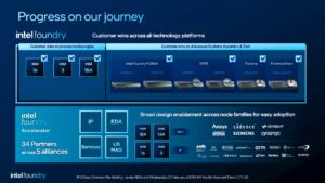
- Figure 3 summarizes Intel’s foundry and packaging capabilities.

Figure 3. Intel’s Foundry and Packaging.
Intel Manufacturing
Also under NDA Keyvan Esfarjani presented Intel’s manufacturing. Key disclosable points are:
- Intel is the only geographically diverse foundry with Fabs in Oregon, Arizona, New Mexico, Ireland and Israel and planned fabs in Ohio and Germany. Intel builds infratsutures around the fabs at each location.
- The IFS foundry model will enable Intel to ramp up processes and keep them in production as opposed to ramping up processes and then ramping them down several years later the way they previously did as an IDM.
- Intel fab locations:
- Fab 28 in Israel is producing i10/i7 and fab 38 is planned for that location.
- Fab 22/32/42 in Arizona are running i10/i7 with fabs 52/62 planned for that site in mid 2025 to run 18A.
- Fab 24 in Ireland is running 14nm with i16 foundry planned, Fab 34/44 also at that location are running i4 now and ramping i3. They will eventually run i3 foundry.
- Fab 9/11x in new Mexico is running advanced packing and will add 65nm with Tower in 2025.
- Planned expansions in Ohio and Germany.
- Oregon wasn’t discussed in any detail presumably because it is a development site although it does do early manufacturing. Oregon has Fabs D1C, D1D and 3 phase of D1X running with rebuilds of D1A and an additional 4th phase of D1X being planned.
Conclusion
Overall, the event was very well executed, and the announcements were impressive. Intel has their process technology development back on track and they are taking foundry seriously and doing the right things to be successful. TSMC is secure as the number one foundry in the world for the foreseeable future, but given Samsung’s recurring yield issues I believe Intel is well positioned to challenge Samsung for the number two position.
Also Read:
ISS 2024 – Logic 2034 – Technology, Economics, and Sustainability
Intel should be the Free World’s Plan A Not Plan B, and we need the US Government to step in
How Disruptive will Chiplets be for Intel and TSMC?
Share this post via:
- SEO Powered Content & PR Distribution. Get Amplified Today.
- PlatoData.Network Vertical Generative Ai. Empower Yourself. Access Here.
- PlatoAiStream. Web3 Intelligence. Knowledge Amplified. Access Here.
- PlatoESG. Carbon, CleanTech, Energy, Environment, Solar, Waste Management. Access Here.
- PlatoHealth. Biotech and Clinical Trials Intelligence. Access Here.
- Source: https://semiwiki.com/events/342309-intel-direct-connect-event/


