By BeomSeok Kim, SeongHwan Kim, Unki Kim, SeongBeom Cho, DongHo Seo, and SangHun Yun
In back-end semiconductor processing it is important to improve the performance of semiconductors due to the limitations of miniaturization in front-end processes. To achieve this goal, the industry continues to invest in back-end processing and competition is fierce in advanced technology of back-end processes. At the same time, 3D semiconductor stacking technology is an important trend in the development of semiconductor packaging. Technologies have been developed, such as the multichip package (MCP) and System in Package (SiP) designs, which put multiple chips in one package. Improvements in packaging technology can accelerate circuit miniaturization in devices used in mobile and wearable products. Miniaturization of circuits means that active as well as passive elements inside the package must be miniaturized. To support advanced designs, a System Level Tester (SLT) was developed that can measure the electrical characteristics of miniaturized passive components and various loads in the package. Specifically, a Capacitance Measurement Unit (CMU) was designed that can measure capacitance and inductance by applying an AC signal. With this unit, it is possible to measure the impedance, capacitance and inductance of active and passive elements as well as composite loads connected pin to pin after packaging.
AMT-9K (System Level Tester)
The developed SLT equipment, the AMT-9K, consists of four function boards. The Parametric Measurement Unit (PMU) analyzes the DC characteristics of semiconductors. Its main function is to apply voltage or current and measure the current or voltage flowing to the device under test (DUT). The Device Power Supply (DPS) has similar functions to the PMU but can apply voltage and high current and can expand the current range using the gang mode. This is mainly used for applying power. The Main ConTroller (MCT) can execute transmitting commands and measurement data from the PMU, DPS and CMU boards to the HOST. In addition, device function tests are performed through interfaces such as I2C and SPI. Finally, the CMU is the function board that is introduced in this paper. It consists of 4-channels and has completely independent channels for the creation of signals and collection of data. The CMU measures AC characteristics, for example impedance, of the DUT. By generating and applying the reference AC source signal (Vx), the Vr signal passing through the DUT is acquired, stored and transmitted. Afterwards, digital signal processing and calculation processing are performed to output the measured value.

Fig. 1: AMT-9K SLT Tester.
CMU hardware design
Measurements are made either with a DC method or an AC method. Development using the DC method has the advantage of lower development cost and less difficulty, but measurement accuracy may be reduced depending on factors such as thermal electromotive force (EMF), lead resistance, leakage current and the dielectric material in the capacitor. The AC method can compensate for these shortcomings and is an efficient method for measuring inductance. The CMU was developed using the AC method and by applying the auto-balancing bridge method. The AC method includes RF I-V method, Network analysis method, Bridge method, Resonant Method and I-V method. However, the auto-balancing bridge method can use a wide frequency band as an AC source and has the advantage of high measurement accuracy. Using this method, it is possible to use 20 Hz to 120 MHz frequencies as an AC source. However, for higher frequencies, it is appropriate to use methods such as RF I-V method.

Fig. 2: DC method and auto-balancing bridge method.
Figure 3 shows a diagram of an equivalent circuit used for CMU development by applying the auto-balancing bridge method. A signal generator, like one using direct digital synthesis (DDS) technology, generates the Vx signal and is applied to the DUT through and operational amplifier (OPAMP). The AC source that passes through the DUT has a phase shift in characteristics. Resistor is in-phase with respect to original signal, capacitors are shifted by -90 degrees and inductors are shifted by +90 degrees. An analog to digital converter (ADC) is used to acquire the Vx signal and Vr signal. An ADC for Vx and Vr is required per CMU channel and the OPAMP is used for the differential input and bias of the ADC. The amplitude of the Vr signal changes depending on the DUT and the range resistor used to match the ADC input level. The developed CMU consists of three range resistors, which determine the measurement range along with the frequency of the AC source and the amplitude of the signal.

Fig. 3: Equivalent circuit of auto-balancing bridge method for CMU.
The circuit was designed and fabricated according to the diagram in figure 3. Figure 4 shows the schematic, artwork and the picture of the actual CMU board. The CMU for the AMT-9K is designed with 4 channels. Considering the noise characteristics, the digital and analog block were separated, and the same circuit blocks were used for each CMU channel. In addition, the patterns were designed to have the same length so there is no difference in the characteristics of each channel.
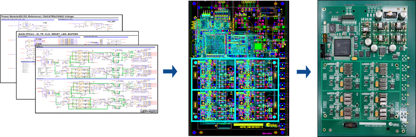
Fig. 4: CMU circuit design.
CMU firmware design
The control of the CMU is divided into three main parts with all information processed through a field-programmable gate array (FPGA). The first part is the signal generator that controls the AC signal generator, digital to analog converter (DAC) and a relay with a selectable range resistor. It uses I2C and SPI protocols to provide this function. The second part is the control of data acquisition. Vx and Vr signals are collected from the ADC and stored in SRAM. It also controls the ROM to store calibration data. The SRAM uses the Memory interface and operates at 400 MB/sec to handle 1.5 Msps data from a total of 8 ADCs. The third is the communication controls. In normal operation, it is combined with the MCT board to send and receive data over SPI. However, it is possible to run the CMU alone without combining with the MCT. The Ethernet module mounted on the CMU is used to connect with the HOST when operating alone, and the HOST is designed to use the same commands used by the MCT.

Fig. 5: CMU control interface.
To exchange information with the HOST, a register map was created that defines the addresses of various control commands. The register map defines all the commands for control, generating signals and the acquisition of data described earlier. For example, to control the amplitude of the AC source to 200 mV, enter the address 0x0000 and the data of 9 to 11 bits as 001 into the Ethernet send function of the HOST. Similarly, the signal generation command can set the frequency and amplitude, and the data acquisition command can set the ADC sampling interval, data number and memory control setting such as data read and write addresses.

Fig. 6: CMU control command.
Figure 7 shows the control flow from the CMU to the signal processing unit through the HOST to measure the impedance. First, the AC source command is sent to generate the signal. Command sets the measurement range by controlling the Range Resistor, which allows the user to: set the frequency and amplitude of the AC signal, set the number and rate of ADC sampling to collect Vx and Vr signals and set the number of data and address to read from the memory where the data is stored. Data between HOST and CMU can be transmitted at about 9 Kbytes per frame using Ethernet and Jumbo Frame settings. The data received from the HOST is analyzed for signal components through a Digital Signal Processing unit and the final results are output.

Fig. 7: CMU measurement control flow.
Digital signal processing
There are three main signal processing units on the HOST. The first receives data, the second extracts features and the third computes parameters. The first data reception is the process of receiving data from the CMU. The CMU consists of a four-channel measurement module and requires two ADCs per channel to acquire the Vx and Vr signals. This means that one CMU requires a total of 8 ADCs, operating in synchronization. Sampling can collect up to 10,000 data points for each of the 8 channels, which means that a maximum of 320 Kbytes can be transferred to the HOST. Second, to extract features, the data collected in the time domain is converted to the frequency domain using the Discrete Fourier Transform (DFT). Extracting the frequency components of the Vx and Vr signals provides the difference and magnitude of the phase angle. Third, one measurement flow ends when each parameter is calculated and displayed according to a known formula.

Fig. 8: DFT computation.
Operating test
A test control program was developed to run the CMU. The test conditions and results are shown in figure 9. In the Operating test result graph, the blue line is the Vx and the orange is Vr. The amount of data in one cycle acquired with a frequency of 100 kHz and 1.5 MHz ADC sampling is 15, and the phase is shifted by about -86.16 degree from the Vr signal due to the characteristics of the capacitor. After processing the DFT data, the extracted result was measured to have an impedance of 1523.33 Ω and a capacitance of 1.0396 nF.
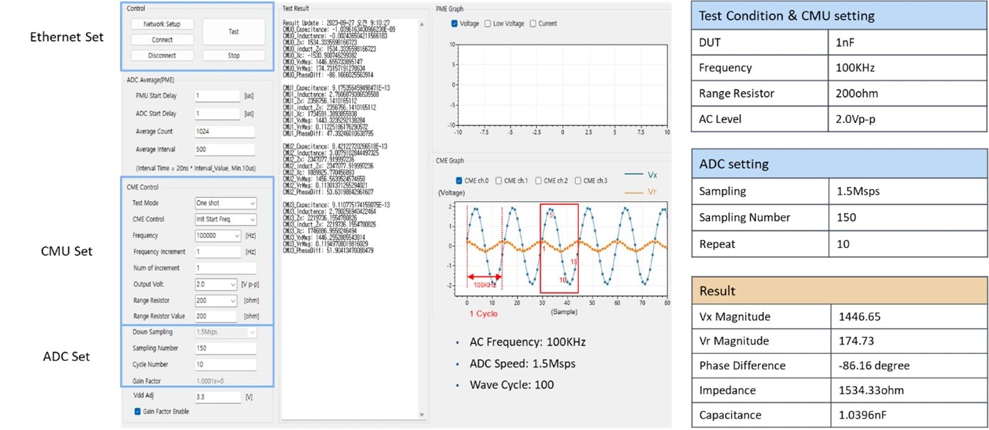
Fig. 9: Operation test.
Compensation
A method is needed to compensate for parasitic components in the circuit and DUT connection cables and measurement paths. Refer to figure 10 and figure 11. The cable from the CMU to the loader board is 1 meter long and runs through a relay to the final DUT. In addition, a tweezer was used to facilitate the manual element. The compensation method is to mount the same resistor value as the range resistor to the DUT, compare it to the original signal, store the difference value (gain factor) and then apply the gain factor to the resulting value of the DUT to be measured. When calculating the gain factor, the conditions of each of the frequency, amplitude and range resistors are swept and stored. The narrower the frequency step, the more accurate the result, but the larger the amount of data.

Fig. 10: Gain factor for compensation.
For example, to obtain the gain factor, a range resistor of 20 kΩ is set and the DUT is also installed with the same 20 kΩ value. Since the installed DUT is a resistive component, the phase difference is close to zero degrees and the magnitude is similar. The gain factor for 4 channels of the CMU is calculated by sweeping 4 amplitudes, 3 range resistors and 1 Hz ~ 100 kHz frequency of the AC source. The measurement showed the gain factor was 1.0137 nF (1.4%) before compensation and improved to 1.00125 nF (0.1%) after.

Fig. 11: Gain factor calculation example.

Fig. 12: Capacitor measurement result (1nF).
Results
Testing was conducted to validate the measurement capability of the CMU against commercial instruments (see figure 13). The measurement DUT is a processor to be applied to automotive applications and the comparison instrument is a commercially available capacitance meter with relatively similar specifications. The tests used the same DUT and were measured 10 times in two states. The instrument conditions were set to be as identical as possible with a frequency of 1 kHz and a signal level of 1V.

Fig. 13: Comparison to measurement time.
The test results (see figure 13) showed that the measurement time was faster than the comparison instrument. The comparison instrument was measured at 380 ms with 1 channel operation, while the CMU of AMT-9K was measured at 837 ms with 4 channels. The ADC sampling number, sampling rate, and meaning of the average of the commercial instrument are not exactly clear.

Fig. 14: Comparison to measurement value.
Measurement accuracy was evaluated for variation by performing 10 repeat measurements in two conditions. As shown in figure 14, in the “Un-press device to socket” condition, the commercial instrument’s Max-Min variation was 13.212 pF and the AMT-9K CMUs was 0.847 pF – a variation for the CMU of only 6%. The variation in “Press device to socket” condition also yielded slightly better results, with 10.634 pF for the CMU compared to 11.580 pF for the commercial device. Figure 15 provides the details of the AMT-9K CMU.

Fig. 15: Specification of AMT-9K CMU.
Summary
As semiconductors become smaller and require higher performance, the complexity of packaging increases, and so does the importance of testers. Various test methods are being explored in the field to respond to issues during production. In fact, capacitance measurements are being discussed as a way to check for cracks in the material inside the packaging and to check for error in the spacing between wires in the wire bonding process. By developing CMUs in-house and mounting them on SLT equipment, miniaturized and multi-channel instruments were designed that increased measurement performance and provided cost benefits. In addition, increased customer satisfaction is expected by actively and timely responding to their technical requirements.
References
- Amkor Device Packages – https://amkor.com/packaging/
- System Level Test (SLT) – https://www.teradyne.com/system-level-test/
- Definition and role of semiconductor package – https://news.skhynix.co.kr/post/seominsuk-column-package-definition
- The Parametric Measurement Handbook – https://www.keysight.com/us/en/assets/7018-05884/application-notes/5992-2508.pdf
- Capacitor Charge and Discharge – https://www.quora.com/Which-are-the-time-constants-of-RL-and-RC-networks
- Novel Processing Routes Neural Interfaces – University of Birmingham, Richard Barrett
SeongHwan Kim, Unki Kim, SeongBeom Cho, DongHo Seo, and SangHun Yun are part of the Test Development Engineering group at Amkor Technology Korea.
- SEO Powered Content & PR Distribution. Get Amplified Today.
- PlatoData.Network Vertical Generative Ai. Empower Yourself. Access Here.
- PlatoAiStream. Web3 Intelligence. Knowledge Amplified. Access Here.
- PlatoESG. Carbon, CleanTech, Energy, Environment, Solar, Waste Management. Access Here.
- PlatoHealth. Biotech and Clinical Trials Intelligence. Access Here.
- Source: https://semiengineering.com/development-of-capacitance-measurement-unit-for-a-system-level-tester/

