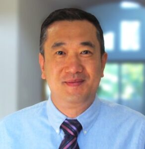
Larry has grown Sarcina from designing semiconductor packages for a few small companies, to doing package designs for top semiconductor companies around the world. From 2014 to 2018, Larry led the expansion of Sarcina beyond package design into final test and wafer sort hardware and software development.
Larry is a semiconductor veteran who started his career at Bell Labs, before moving on to DEC, Intel, and TSMC. Along the way he developed a proven track record of delivering successful products including the Alpha, Itanium 2, Pentium 4, and XBOX 360 microprocessors. Over his career, he has tapped out nearly 1,000 packages with a greater than 99% first tape-out success rate.
Larry received his B.S. in Physics from Peking University and his Ph.D. in Electrical & Computer Engineering from Rutgers University. He has many refereed IEEE publications and holds multiple U.S. patents which have been used in leading US companies’ key products.
Tell us about your company?
Sarcina was founded in Palo Alto, CA in October of 2011. The name “Sarcina” refers to the backpack carried by Roman soldiers. Although it didn’t include their arms and armor, Sarcinas provided the essentials for daily living necessary to accomplish their military missions.
We are an Application Specific Advanced Package (ASAP) company that provides integrated WIPO (Wafer-In, Product-Out) services to customers around the globe. Our vision is to be the leading post-silicon service, setting standards for excellence by providing high-quality, dependable, creative, and assured package, test, and production services to our customers.
What problems are you solving?
As the complexity of designing an advanced semiconductor package becomes more challenging, and the cost of sustaining an internal packaging team for small to mid-sized chip companies and system companies becomes less economical, outsourcing chip packaging makes more sense for many ASIC and system companies. Companies often have to work with multiple independent vendors in Asia to accomplish most of their post-silicon tasks. So, outsourcing these tasks makes sense. That’s why we formed Sarcina: to meet these specific demands.
What application areas are your strongest?
We are the experts in high-power, high pin-count, and high data rate semiconductor packages for high-performance computing applications. Our 100% right-the-first-time success substantiates this claim.
What keeps your customers up at night?
Unresolved technical problems and missed deadlines.
We understand these two pain points. Either one causes companies to work double-shifts: one for their regular day job and the other at night to fix past mistakes. Sarcina’s job is to make sure that never happens and to make working with Sarcina a seamless, time-saving process.
What Does the Competitive Landscape Look Like, and How Do You Differentiate?
That’s an interesting question, and you may find the answer surprising. If you look at this from a service perspective, you’d think we have a large number of competitors across a broad swath of the semiconductor value chain: wafer foundries, ASIC companies, OSAT (Outsourced Semiconductor Assembly and Test) houses. However, if you view this from a business problem-solving perspective, the ASAP space is unique.
We solve both technical and business problems for small to mid-sized ASIC companies and system houses with understaffed post-silicon teams. Our value proposition is advanced packaging, test, assembly, and production at cost points lower than what can be achieved in-house. In the packaging area, our biggest competitors are the low-cost, low-tech, and mature technology entities.
Fortunately, with the boom of AI, mobile devices, autonomous driving, IoT, and the desire to win tomorrow’s tech wars, the market has expanded significantly. We believe the market is large enough to accommodate all of these players. Over time, the inefficient small players may drop out of the race.
Sarcina’s strength and fundamental differentiation is our ability to complete high-performance engineering projects. Over the past 12 years, Sarcina has taped out more than 100 packages, all first-time successes. We’ve never re-taped out a single package. At the same time, we’re able to complete advanced projects with a fraction of the headcount required by other companies. Our engineering efficiency is several times that of the industry norm.
In the networking business, there is a famous rule of thumb: if your product can offer a 10X performance increase … such as speed, efficiency, or capability …. but costs only 2X as much as the existing solution, your business will take off. In our business, we believe that if our engineering efficiency is several times that of our competitor, we’ll effectively compete, regardless of the size of the competitor.
What New Features/Technology Are You Working On?
Every four years, SerDes and PCIe data rates double, and DDR technology advances by a generation. Today, people are working on 112 Gb/s and 224 Gb/s PAM4 SerDes; 32 Gb/s NRZ PCIe-5 and 64 Gb/s PAM4 PCIe-6, as well as 6400 Mb/s to ~10 Gb/s LPDDR5/DDR5/GDDR6. Sarcina’s package design technology is ready for these high data rate chips in an HVM (High Volume Manufacture) environment. IP companies usually provide a live demo of their highest data rate IP with a few lanes of data communication. In a real chip, there will be many lanes with limited routing space. Our job is to provide the package design that meets our customers’ data rate requirements for their real chips. As of today, Sarcina has designed packages for 112 Gb/s SerDes, 64 Gb/s PCIe-6, and 6.4 Gb/s LPDDR5. Our next task is 224 Gb/s PAM4 SerDes with approximately 100 lanes of data communication inside a single package. We are also supporting these data rates on our final test loadboard loopback test.
How Do Customers Normally Engage With Your Company?
Surprisingly, word-of-mouth remains our most efficient way to land business. However, we are stepping up our overall industry presence and visibility as the demand for advanced technology packaging expands. We’re investing more in building collaborations with technology partners and implementing multiple one-on-one outreach channels. While businesses still value face-to-face meetings, we’ve significantly expanded our marketing campaign and assets. We’re appearing at more trade shows, ramping up our earned and paid media, and rebuilding our website, while refreshing our brand assets. All these efforts have dramatically increased our company’s visibility, opening doors to more advanced technology decision-makers.
Also Read:
CEO Interview: Vincent Bligny of Aniah
CEO Interview: Jay Dawani of Lemurian Labs
Luc Burgun: EDA CEO, Now French Startup Investor
Share this post via:
- SEO Powered Content & PR Distribution. Get Amplified Today.
- PlatoData.Network Vertical Generative Ai. Empower Yourself. Access Here.
- PlatoAiStream. Web3 Intelligence. Knowledge Amplified. Access Here.
- PlatoESG. Carbon, CleanTech, Energy, Environment, Solar, Waste Management. Access Here.
- PlatoHealth. Biotech and Clinical Trials Intelligence. Access Here.
- Source: https://semiwiki.com/ceo-interviews/342372-ceo-interview-larry-zu-of-sarcina-technology/


