Home > Press > TUS researchers propose a simple, inexpensive approach to fabricating carbon nanotube wiring on plastic films: The proposed method produces wiring suitable for developing all-carbon devices, including flexible sensors and energy conversion and storage devices
 |
| A novel method proposed by TUS researchers for the fabrication of multi-walled carbon nanotubes on flexible substrates, such as plastic films, eliminates many of the drawbacks of conventional techniques and can be used to mass-produce carbon wiring for flexible all-carbon electronic devices. CREDIT Takashi Ikuno from TUS, Japan |
Abstract:
Carbon nanotubes (CNTs) are cylindrical tube-like structures made of carbon atoms that display highly desirable physical properties like high strength, low weight, and excellent thermal and electrical conductivities. This makes them ideal materials for various applications, including reinforcement materials, energy storage and conversion devices, and electronics. Despite such immense potential, however, there have been challenges in commercializing CNTs, such as their incorporation on plastic substrates for fabricating flexible CNT-based devices. Traditional fabrication methods require carefully controlled environments such as high temperatures and a clean room. Further, they require repeat transfers to produce CNTs with different resistance values.
TUS researchers propose a simple, inexpensive approach to fabricating carbon nanotube wiring on plastic films: The proposed method produces wiring suitable for developing all-carbon devices, including flexible sensors and energy conversion and storage devices
Tokyo, Japan | Posted on March 3rd, 2023
More direct methods such as laser-induced forward transfer (LIFT) and thermal fusion (TF) have been developed as alternatives. In the LIFT method, a laser is used to directly transfer CNTs onto substrates, while in TF, CNTs are mixed with polymers that are then selectively removed by a laser to form CNT wires with varying resistance values. However, both these methods are expensive and have their unique problems. LIFT requires expensive pulsed lasers and preparation of CNTs with specific resistance values, while TF uses large amounts of CNTs that are not utilized and go to waste.
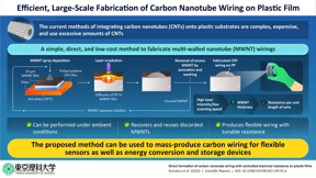
Aiming to develop a more simple and inexpensive approach, Associate Professor Dr. Takashi Ikuno along with his collaborators, Mr. Hiroaki Komatsu, Mr. Yosuke Sugita and Mr. Takahiro Matsunami at Tokyo University of Science, Japan, recently proposed a novel method that enables fabrication of multi-walled CNT (MWNT) wiring on a plastic film under ambient conditions (room temperature and atmospheric pressure) using a low-cost laser.
The breakthrough, published in the journal Scientific Reports on 08 February 2023, involves coating a polypropylene (PP) film with an MWNT film about 10 μm thick and then exposing it to a mW UV laser. The result is a conductive wiring made of a combination of MWNT and PP.
“This process enables the easy ‘drawing’ of wiring and flexible devices for wearable sensors without the need for complex processes,” highlights Dr. Ikuno.
The researchers attributed the formation of these wires to the difference in the thermal conductivities between the MWNT and the PP film. As the MWNT/PP film is exposed to the laser, the high thermal conductivity of the MWNT layer causes the heat to spread along the length of the wire, resulting in high temperatures at the MWNT–PP interface and lower temperatures elsewhere in the PP film. Directly below the laser, where temperatures are the highest, the PP diffuses into the MWNT film to form a thick PP/MWNT composite, while a thin PP/MWNT layer is formed at the edges of the laser where temperatures are relatively low.
The proposed method also allows the fabrication of carbon wires with different resistance values within the same process (without repeat transfer) by simply changing the irradiation conditions, thereby eliminating the need for additional steps. Exposing the PP/MWNT film to high laser energies, achieved either by low scanning speeds, a high number of laser exposures, or the use of a high-powered laser, produces thicker wires with a higher concentration of MWNTs. Consequently, the lower resistivity of MWNT and the thicker wire lowers the resistance per unit length of the wire (resistance is directly proportional to the ratio between the resistivity and the thickness of the wire).
By precisely controlling the exposure of the MWNT/PP film to laser light, the researchers successfully fabricated MWNT wires with a wide range of resistance values, from 0.789 kΩ/cm to 114 kΩ/cm. Moreover, these wires were highly flexible and maintained their resistance even when bent repeatedly.
Additionally, the method solved one of the pressing issues with current techniques, namely the inability of LIFT and TF techniques to reuse CNTs not utilized in the fabrication process. In the proposed method, MWNTs not incorporated into the PP film during laser irradiation can be recovered and reused, allowing for the creation of new MWNT wires with little to no change in resistance values.
With its simplicity, efficient utilization of CNTs, and the capability to create high-quality wires, the new method has the potential to realize large-scale manufacturing of flexible carbon wiring for flexible sensors and energy conversion and storage devices.
“We expect the process cost to be significantly reduced compared to that for conventional methods. This, in turn, will contribute to the realization of low-cost flexible sensors that are expected to have wide applications in large quantities,” concludes Dr. Ikuno.
####
About Tokyo University of Science
Tokyo University of Science (TUS) is a well-known and respected university, and the largest science-specialized private research university in Japan, with four campuses in central Tokyo and its suburbs and in Hokkaido. Established in 1881, the university has continually contributed to Japan’s development in science through inculcating the love for science in researchers, technicians, and educators.
With a mission of “Creating science and technology for the harmonious development of nature, human beings, and society,” TUS has undertaken a wide range of research from basic to applied science. TUS has embraced a multidisciplinary approach to research and undertaken intensive study in some of today’s most vital fields. TUS is a meritocracy where the best in science is recognized and nurtured. It is the only private university in Japan that has produced a Nobel Prize winner and the only private university in Asia to produce Nobel Prize winners within the natural sciences field.
Website: https://www.tus.ac.jp/en/mediarelations/
About Associate Professor Takashi Ikuno from Tokyo University of Science
Takashi Ikuno received his Ph.D. degree from Osaka University, whereupon he worked at the Lawrence Berkeley National Laboratory and UC Berkeley, USA as a postdoctoral researcher and later at Toyota Central R&D Labs as a senior researcher. He currently works as an Associate Professor in the Department of Applied Electronics at Tokyo University of Science (TUS), Japan. His research interests include developing electronic devices with nanocarbon and low-dimensional nanomaterials. He can be reached at
Funding information
This work was partly supported by Grant-in-Aid for Scientific Research (C)(22K04880) from Japan Society for the Promotion of Science, MEXT, and the “Advanced Research Infrastructure for Materials and Nanotechnology in Japan (ARIM)” of the Ministry of Education, Culture, Sports, Science and Technology (MEXT). Proposal Number JPMXP1222NM0102.
For more information, please click here
Contacts:
Hiroshi Matsuda
Tokyo University of Science
Expert Contact
Professor Takashi Ikuno
Tokyo University of Science
Copyright © Tokyo University of Science
If you have a comment, please Contact us.
Issuers of news releases, not 7th Wave, Inc. or Nanotechnology Now, are solely responsible for the accuracy of the content.
Bookmark:


| Related Links |
| Related News Press |
News and information
![]() Scientists push the boundaries of manipulating light at the submicroscopic level March 3rd, 2023
Scientists push the boundaries of manipulating light at the submicroscopic level March 3rd, 2023
![]() Lipid nanoparticles highly effective in gene therapy March 3rd, 2023
Lipid nanoparticles highly effective in gene therapy March 3rd, 2023
Possible Futures
![]() Scientists develop self-tunable electro-mechano responsive elastomers March 3rd, 2023
Scientists develop self-tunable electro-mechano responsive elastomers March 3rd, 2023
![]() Recent progress of carbon-based non-noble metal single-atom catalysts for energy conversion electrocatalysis March 3rd, 2023
Recent progress of carbon-based non-noble metal single-atom catalysts for energy conversion electrocatalysis March 3rd, 2023
Memory Technology
![]() Approaching the terahertz regime: Room temperature quantum magnets switch states trillions of times per second January 20th, 2023
Approaching the terahertz regime: Room temperature quantum magnets switch states trillions of times per second January 20th, 2023
![]() Scientists unravel ‘Hall effect’ mystery in search for next generation memory storage devices August 19th, 2022
Scientists unravel ‘Hall effect’ mystery in search for next generation memory storage devices August 19th, 2022
Nanotubes/Buckyballs/Fullerenes/Nanorods
![]() Current and Future Developments in Nanomaterials and Carbon Nanotubes: Applications of Nanomaterials in Energy Storage and Electronics October 28th, 2022
Current and Future Developments in Nanomaterials and Carbon Nanotubes: Applications of Nanomaterials in Energy Storage and Electronics October 28th, 2022
![]() Buckyballs on gold are less exotic than graphene July 22nd, 2022
Buckyballs on gold are less exotic than graphene July 22nd, 2022
![]() Strain-sensing smart skin ready to deploy: Nanotube-embedded coating detects threats from wear and tear in large structures July 15th, 2022
Strain-sensing smart skin ready to deploy: Nanotube-embedded coating detects threats from wear and tear in large structures July 15th, 2022
![]() Boron nitride nanotube fibers get real: Rice lab creates first heat-tolerant, stable fibers from wet-spinning process June 24th, 2022
Boron nitride nanotube fibers get real: Rice lab creates first heat-tolerant, stable fibers from wet-spinning process June 24th, 2022
Sensors
![]() Scientists push the boundaries of manipulating light at the submicroscopic level March 3rd, 2023
Scientists push the boundaries of manipulating light at the submicroscopic level March 3rd, 2023
![]() New nanowire sensors are the next step in the Internet of Things January 6th, 2023
New nanowire sensors are the next step in the Internet of Things January 6th, 2023
Discoveries
![]() Scientists develop self-tunable electro-mechano responsive elastomers March 3rd, 2023
Scientists develop self-tunable electro-mechano responsive elastomers March 3rd, 2023
![]() Recent progress of carbon-based non-noble metal single-atom catalysts for energy conversion electrocatalysis March 3rd, 2023
Recent progress of carbon-based non-noble metal single-atom catalysts for energy conversion electrocatalysis March 3rd, 2023
Announcements
![]() Recent progress of carbon-based non-noble metal single-atom catalysts for energy conversion electrocatalysis March 3rd, 2023
Recent progress of carbon-based non-noble metal single-atom catalysts for energy conversion electrocatalysis March 3rd, 2023
![]() Getting drugs across the blood-brain barrier using nanoparticles March 3rd, 2023
Getting drugs across the blood-brain barrier using nanoparticles March 3rd, 2023
Interviews/Book Reviews/Essays/Reports/Podcasts/Journals/White papers/Posters
![]() Recent progress of carbon-based non-noble metal single-atom catalysts for energy conversion electrocatalysis March 3rd, 2023
Recent progress of carbon-based non-noble metal single-atom catalysts for energy conversion electrocatalysis March 3rd, 2023
![]() Getting drugs across the blood-brain barrier using nanoparticles March 3rd, 2023
Getting drugs across the blood-brain barrier using nanoparticles March 3rd, 2023
Energy
![]() Make them thin enough, and antiferroelectric materials become ferroelectric February 10th, 2023
Make them thin enough, and antiferroelectric materials become ferroelectric February 10th, 2023
![]() Stability of perovskite solar cells reaches next milestone January 27th, 2023
Stability of perovskite solar cells reaches next milestone January 27th, 2023
![]() Temperature-sensing building material changes color to save energy January 27th, 2023
Temperature-sensing building material changes color to save energy January 27th, 2023
- SEO Powered Content & PR Distribution. Get Amplified Today.
- Platoblockchain. Web3 Metaverse Intelligence. Knowledge Amplified. Access Here.
- Source: http://www.nanotech-now.com/news.cgi?story_id=57307

