Ionic circuit for neural nets
Researchers at Harvard University and DNA Script developed an ionic circuit comprising hundreds of ionic transistors for neural net computing.
While ions in water move slower than electrons in semiconductors, the team noted that the diversity of ionic species with different physical and chemical properties could be harnessed for more diverse information processing.
The researchers built a new type of ionic transistor consisting of an aqueous solution of quinone molecules, interfaced with two concentric ring electrodes with a center disk electrode, like a bullseye. The two ring electrodes electrochemically lower and tune the local pH around the center disk by producing and trapping hydrogen ions. A voltage applied to the center disk causes an electrochemical reaction to generate an ionic current from the disk into the water. The reaction rate can be sped up or down –– increasing or decreasing the ionic current — by tuning the local pH. In other words, the pH gates the disk’s ionic current in the aqueous solution, creating an ionic counterpart of the electronic transistor.
![]()
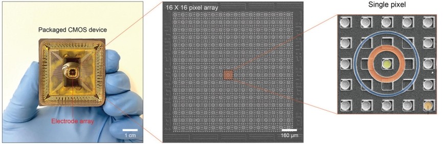
A CMOS chip (left) with an array (center) of hundreds of individual ionic transistors (right). (Credit: Woo-Bin Jung/Harvard SEAS)
They then engineered the pH-gated ionic transistor in such a way that the disk current is an arithmetic multiplication of the disk voltage and a “weight” parameter representing the local pH gating the transistor. They organized these transistors into a 16 × 16 array to expand the analog arithmetic multiplication of individual transistors into an analog matrix multiplication, with the array of local pH values serving as a weight matrix encountered in neural networks.
“Matrix multiplication is the most prevalent calculation in neural networks for artificial intelligence,” said Woo-Bin Jung, a postdoctoral fellow at Harvard John A. Paulson School of Engineering and Applied Sciences (SEAS). “Our ionic circuit performs the matrix multiplication in water in an analog manner that is based fully on electrochemical machinery.”
“Microprocessors manipulate electrons in a digital fashion to perform matrix multiplication,” said Donhee Ham, professor of electrical engineering and applied physics at SEAS. “While our ionic circuit cannot be as fast or accurate as the digital microprocessors, the electrochemical matrix multiplication in water is charming in its own right, and has a potential to be energy efficient.”
Jung added that the team plans to enrich the chemical complexity of the system. “So far, we have used only 3 to 4 ionic species, such as hydrogen and quinone ions, to enable the gating and ionic transport in the aqueous ionic transistor,” said Jung. “It will be very interesting to employ more diverse ionic species and to see how we can exploit them to make rich the contents of information to be processed.”
3D printing MEMS sensors
Researchers from KTH Royal Institute of Technology, École Polytechnique Fédérale de Lausanne (EPFL), and Hochschule Kaiserslautern University of Applied Sciences propose using 3D printing to create custom MEMS sensors in smaller volumes.
“The costs of manufacturing process development and device design optimizations do not scale down for lower production volumes,” said Frank Niklaus of the KTH Royal Institute of Technology, leaving engineers with a choice of suboptimal off-the-shelf MEMS devices or economically unviable start-up costs.
The researchers point to accelerometers for aircraft and vibration sensors for industrial machinery as two types of MEMS sensors that could benefit from customization but have low volumes.
“The researchers built on a process called two-photon polymerization, which can produce high resolution objects as small as few hundreds of nanometers in size, but not capable of sensing functionality,” explained KTH’s David Callahan. “To form the transducing elements, the method uses a technique called shadow-masking, which works something like a stencil. On the 3D-printed structure they fabricate features with a T-shaped cross-section, which work like umbrellas. They then deposit metal from above, and as a result, the sides of the T-shaped features are not coated with the metal. This means the metal on the top of the T is electrically isolated from the rest of the structure.”
The method can be used to manufacture a dozen or so custom designed MEMS accelerometers in a few hours, which the researchers said could provide an economically viable way to prototype MEMS devices and manufacture small- and medium-sized batches of tens of thousands to a few thousand MEMS sensors per year.
“This is something that has not been possible until now, because the start-up costs for manufacturing a MEMS product using conventional semiconductor technology are on the order of hundreds of thousands of dollars and the lead times are several months or more,” said Niklaus. “The new capabilities offered by 3D-printed MEMS could result in a new paradigm in MEMS and sensor manufacturing.”
Quantum bus
Physicists from Forschungszentrum Jülich and RWTH Aachen University succeeded in transferring electrons, the carriers of quantum information in semiconductor spin-based quantum systems, over several micrometers on a quantum chip, a step they said could lead to systems with millions of qubits.
“Currently, each individual qubit is connected via several signal lines to control units about the size of a cupboard. That still works for a few qubits. But it no longer makes sense if you want to put millions of qubits on the chip. Because that’s necessary for quantum error correction,” said Lars Schreiber from the JARA Institute for Quantum Information at Forschungszentrum Jülich and RWTH Aachen University.
Ultimately, they aim to integrate parts of the control electronics directly on the chip.
“The natural entanglement that is caused by the proximity of the particles alone is limited to a very small range, about 100 nanometers. To couple the qubits, they currently have to be placed very close to each other. There is simply no space for additional control electronics that we would like to install there,” said Schreiber.


Semiconductor quantum chip with quantum bus of the JARA cooperation of Forschungszentrum Jülich and RWTH Aachen University. (Credit: Forschungszentrum Jülich / Sascha Kreklau)
The team’s quantum bus helps exchange quantum information between the qubits over greater distances, based on a new way of transporting electrons. “Until now, people have tried to steer the electrons specifically around individual disturbances on their path. Or they created a series of so-called quantum dots and let the electrons hop from one of these dots to another. Both approaches require precise signal adjustment, which results in too complex control electronics,” explained Schreiber. “In contrast, we generate a potential wave on which the electrons simply surf over various sources of interference. A few control signals are sufficient for such a uniform wave; four sinusoidal pulses is all it takes.”
“About 10 micrometers have to be bridged from one qubit to the next. According to theory, millions of qubits can be realized with such an architecture,” said Hendrik Bluhm, professor and IQI Institute director.
As a next step, the physicists want to show that the qubit information encoded in the electron spin is not lost during transportation. Theoretical calculations have shown that this is possible in silicon in certain speed ranges.
- SEO Powered Content & PR Distribution. Get Amplified Today.
- Platoblockchain. Web3 Metaverse Intelligence. Knowledge Amplified. Access Here.
- Source: https://semiengineering.com/research-bits-jan-17/

