Home > Press > Graphene grows – and we can see it
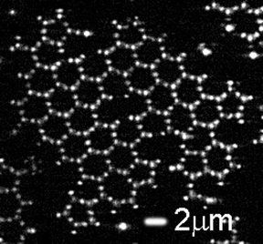 |
| Pieces of a graphene lattice made from patchy particles. Because the particles can be followed one-by-one, defects can be studied at the particle scale. Image: Swinkels et al. CREDIT Swinkels et al |
Abstract:
Graphene is the strongest of all materials. On top of that, it is exceptionally good at conducting heat and electrical currents, making it one of the most special and versatile materials we know. For all these reasons, the discovery of graphene was awarded the Nobel Prize in Physics in 2010. Yet, many properties of the material and its cousins are still poorly understood – for the simple reason that the atoms they are made up of are very difficult to observe. A team of researchers from the University of Amsterdam and New York University have now found a surprising way to solve this issue.
Graphene grows – and we can see it
Amsterdam, Netherlands | Posted on March 24th, 2023
Two-dimensional materials, consisting of a hyper-thin single layer of atomic crystal, have attracted a lot of attention recently. This well-deserved attention is mainly due to their unusual properties, very different from their three-dimensional ‘bulk’ counterparts. Graphene, the most famous representative, and many other two-dimensional materials, are nowadays researched intensely in the laboratory. Perhaps surprisingly, crucial to the special properties of these materials are defects, locations where the crystal structure is not perfect. There, the ordered arrangement of the layer of atoms is disturbed and the coordination of atoms changes locally.
Visualizing atoms
Despite the fact that defects have been shown to be crucial for a material’s properties, and they are almost always either present or added on purpose, not much is known about how they form and how they evolve in time. The reason for this is simple: atoms are just too small and move too fast to directly follow them.
In an effort to make the defects in graphene-like materials observable, the team of researchers, from the UvA-Institute of Physics and New York University, found a way to build micrometre-size models of atomic graphene. To achieve this, they used so-called ‘patchy particles’. These particles – large enough to be easily visible in a microscope, yet small enough to reproduce many of the properties of actual atoms – interact with the same coordination as atoms in graphene, and form the same structure. The researchers built a model system and used it to obtain insight into defects, their formation and evolution with time. Their results were published in Nature Communications this week.
Building graphene
Graphene is made up of carbon atoms that each have three neighbours, arranged in the well-known ‘honeycomb’ structure. It is this special structure that lends graphene its unique mechanical and electronic properties. To achieve the same structure in their model, the researchers used tiny particles made of polystyrene, decorated with three even tinier patches of a material known as 3-(trimethoxysilyl)propyl – or TPM for short. The configuration of the TPM patches mimicked the coordination of carbon atoms in the graphene lattice. The researchers then made the patches attractive so that the particles could form bonds with each other, again in analogy with the carbon atoms in graphene.
After being left alone for a few hours, when observed under a microscope the ‘mock carbon’ particles turned out to indeed arrange themselves into a honeycomb lattice. The researchers then looked in more detail at defects in the model graphene lattice. They observed that also in this respect the model worked: it showed characteristic defect motifs that are also known from atomic graphene. Contrary to real graphene, the direct observation and long formation time of the model now allowed the physicists to follow these defects from the very start of their formation, up to the integration into the lattice.
Unexpected results
The new look at the growth of graphene-like materials immediately led to new knowledge about these two-dimensional structures. Unexpectedly, the researchers found that the most common type of defect already forms in the very initial stages of growth, when the lattice is not yet established. They also observed how the lattice mismatch is then ‘repaired’ by another defect, leading to a stable defect configuration, which either remains or only very slowly heals further to a more perfect lattice.
Thus, the model system not only allows to rebuild the graphene lattice on a larger scale for all sorts of applications, but the direct observations also allow insights into atomic dynamics in this class of materials. As defects are central to the properties of all atomically thin materials, these direct observations in model systems help further engineer the atomic counterparts, for example for applications in ultra-lightweight materials and optical and electronic devices.
####
For more information, please click here
Contacts:
Laura Erdtsieck
Universiteit van Amsterdam
Office: 0031-205-252-695
Copyright © Universiteit van Amsterdam
If you have a comment, please Contact us.
Issuers of news releases, not 7th Wave, Inc. or Nanotechnology Now, are solely responsible for the accuracy of the content.
Bookmark:


| Related Links |
| Related News Press |
2 Dimensional Materials
![]() HKUMed invents a novel two-dimensional (2D) ultrasound-responsive antibacterial nano-sheets to effectively address bone tissue infection March 24th, 2023
HKUMed invents a novel two-dimensional (2D) ultrasound-responsive antibacterial nano-sheets to effectively address bone tissue infection March 24th, 2023
![]() New study opens the door to ultrafast 2D devices that use nonequilibrium exciton superdiffusion February 10th, 2023
New study opens the door to ultrafast 2D devices that use nonequilibrium exciton superdiffusion February 10th, 2023
![]() Wafer-scale 2D MoTe₂ layers enable highly-sensitive broadband integrated infrared detector January 6th, 2023
Wafer-scale 2D MoTe₂ layers enable highly-sensitive broadband integrated infrared detector January 6th, 2023
News and information
![]() Optical switching at record speeds opens door for ultrafast, light-based electronics and computers: March 24th, 2023
Optical switching at record speeds opens door for ultrafast, light-based electronics and computers: March 24th, 2023
![]() Robot caterpillar demonstrates new approach to locomotion for soft robotics March 24th, 2023
Robot caterpillar demonstrates new approach to locomotion for soft robotics March 24th, 2023
![]() Semiconductor lattice marries electrons and magnetic moments March 24th, 2023
Semiconductor lattice marries electrons and magnetic moments March 24th, 2023
![]() Light meets deep learning: computing fast enough for next-gen AI March 24th, 2023
Light meets deep learning: computing fast enough for next-gen AI March 24th, 2023
Graphene/ Graphite
![]() Graphene Flagship start-up Bedimensional closes a second €10 million investment round February 10th, 2023
Graphene Flagship start-up Bedimensional closes a second €10 million investment round February 10th, 2023
Possible Futures
![]() New experiment translates quantum information between technologies in an important step for the quantum internet March 24th, 2023
New experiment translates quantum information between technologies in an important step for the quantum internet March 24th, 2023
![]() HKUMed invents a novel two-dimensional (2D) ultrasound-responsive antibacterial nano-sheets to effectively address bone tissue infection March 24th, 2023
HKUMed invents a novel two-dimensional (2D) ultrasound-responsive antibacterial nano-sheets to effectively address bone tissue infection March 24th, 2023
![]() A universal HCl-assistant powder-to-powder strategy for preparing lead-free perovskites March 24th, 2023
A universal HCl-assistant powder-to-powder strategy for preparing lead-free perovskites March 24th, 2023
![]() Optical switching at record speeds opens door for ultrafast, light-based electronics and computers: March 24th, 2023
Optical switching at record speeds opens door for ultrafast, light-based electronics and computers: March 24th, 2023
Chip Technology
![]() Optical switching at record speeds opens door for ultrafast, light-based electronics and computers: March 24th, 2023
Optical switching at record speeds opens door for ultrafast, light-based electronics and computers: March 24th, 2023
![]() Semiconductor lattice marries electrons and magnetic moments March 24th, 2023
Semiconductor lattice marries electrons and magnetic moments March 24th, 2023
![]() Light meets deep learning: computing fast enough for next-gen AI March 24th, 2023
Light meets deep learning: computing fast enough for next-gen AI March 24th, 2023
Discoveries
![]() New experiment translates quantum information between technologies in an important step for the quantum internet March 24th, 2023
New experiment translates quantum information between technologies in an important step for the quantum internet March 24th, 2023
![]() HKUMed invents a novel two-dimensional (2D) ultrasound-responsive antibacterial nano-sheets to effectively address bone tissue infection March 24th, 2023
HKUMed invents a novel two-dimensional (2D) ultrasound-responsive antibacterial nano-sheets to effectively address bone tissue infection March 24th, 2023
![]() A universal HCl-assistant powder-to-powder strategy for preparing lead-free perovskites March 24th, 2023
A universal HCl-assistant powder-to-powder strategy for preparing lead-free perovskites March 24th, 2023
![]() Optical switching at record speeds opens door for ultrafast, light-based electronics and computers: March 24th, 2023
Optical switching at record speeds opens door for ultrafast, light-based electronics and computers: March 24th, 2023
Materials/Metamaterials
![]() A universal HCl-assistant powder-to-powder strategy for preparing lead-free perovskites March 24th, 2023
A universal HCl-assistant powder-to-powder strategy for preparing lead-free perovskites March 24th, 2023
![]() Bilayer PET/PVDF substrate-reinforced solid polymer electrolyte improves solid-state lithium metal battery performance March 24th, 2023
Bilayer PET/PVDF substrate-reinforced solid polymer electrolyte improves solid-state lithium metal battery performance March 24th, 2023
![]() Understanding the mechanism of non-uniform formation of diamond film on tools: Paving the way to a dry process with less environmental impact March 24th, 2023
Understanding the mechanism of non-uniform formation of diamond film on tools: Paving the way to a dry process with less environmental impact March 24th, 2023
![]() Scientists develop self-tunable electro-mechano responsive elastomers March 3rd, 2023
Scientists develop self-tunable electro-mechano responsive elastomers March 3rd, 2023
Announcements
![]() Robot caterpillar demonstrates new approach to locomotion for soft robotics March 24th, 2023
Robot caterpillar demonstrates new approach to locomotion for soft robotics March 24th, 2023
![]() Semiconductor lattice marries electrons and magnetic moments March 24th, 2023
Semiconductor lattice marries electrons and magnetic moments March 24th, 2023
![]() Light meets deep learning: computing fast enough for next-gen AI March 24th, 2023
Light meets deep learning: computing fast enough for next-gen AI March 24th, 2023
![]() Bilayer PET/PVDF substrate-reinforced solid polymer electrolyte improves solid-state lithium metal battery performance March 24th, 2023
Bilayer PET/PVDF substrate-reinforced solid polymer electrolyte improves solid-state lithium metal battery performance March 24th, 2023
Interviews/Book Reviews/Essays/Reports/Podcasts/Journals/White papers/Posters
![]() HKUMed invents a novel two-dimensional (2D) ultrasound-responsive antibacterial nano-sheets to effectively address bone tissue infection March 24th, 2023
HKUMed invents a novel two-dimensional (2D) ultrasound-responsive antibacterial nano-sheets to effectively address bone tissue infection March 24th, 2023
![]() A universal HCl-assistant powder-to-powder strategy for preparing lead-free perovskites March 24th, 2023
A universal HCl-assistant powder-to-powder strategy for preparing lead-free perovskites March 24th, 2023
![]() Optical switching at record speeds opens door for ultrafast, light-based electronics and computers: March 24th, 2023
Optical switching at record speeds opens door for ultrafast, light-based electronics and computers: March 24th, 2023
![]() Robot caterpillar demonstrates new approach to locomotion for soft robotics March 24th, 2023
Robot caterpillar demonstrates new approach to locomotion for soft robotics March 24th, 2023
- SEO Powered Content & PR Distribution. Get Amplified Today.
- Platoblockchain. Web3 Metaverse Intelligence. Knowledge Amplified. Access Here.
- Source: http://www.nanotech-now.com/news.cgi?story_id=57323

