| Dec 27, 2023 |
|
|
|
(Nanowerk Spotlight) Researchers have long sought to maximize the efficiency of perovskite solar cells while minimizing production costs. Thinner solar cell films enable low-cost production but limit efficiency. Thicker films boost efficiency but are prone to defects that undermine performance. However, prior attempts at micron-scale perovskite films suffered notable declines in fill factor and voltage. Thereby limiting their efficiency potential. Striking an optimal balance between thickness and efficiency has proven an enduring challenge.
|
|
Recent innovations in materials and manufacturing have brought perovskite solar cells to the cusp of commercial viability. Efficiencies now rival traditional silicon cells while requiring far less energy and cost to produce. However, wider adoption depends on improving performance and stability while retaining economical fabrication techniques.
|
|
New work by a team at Forschungszentrum Jülich in Germany, reported in Advanced Energy Materials (“Hole Transporting Bilayers for Efficient Micrometer-Thick Perovskite Solar Cells”), fundamentally recognizes the critical role transport layers play in exacerbating thickness-dependent losses. Even with perfect absorber mobility/lifetimes. By optimizing a dual-layer hole transport architecture to reduce resistive losses and recombination, the authors achieve remarkable efficiency retention at over 1 micron thickness.
|
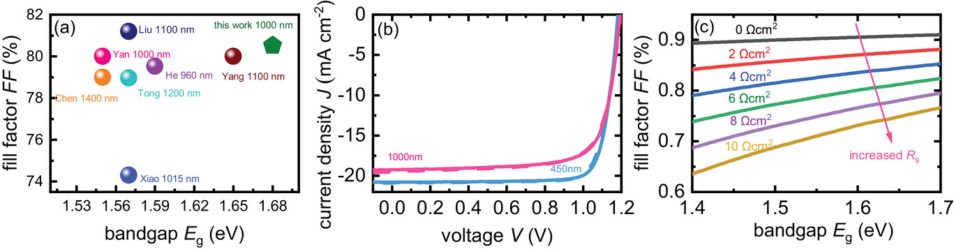 |
| a) Comparison of the FF and the corresponding perovskite film thickness and bandgap in the representative reports and this work. b) Illuminated J–V curves of perovskite solar cells with different thicknesses based on Me-4PACz, the cell performance parameters are listed in Table S1, Supporting Information. c) Fill factor as a function of the bandgap according to Equation (1) considering different resistances. (© Wiley-VCH Verlag)
|
|
This research centers on an ingenious solar cell architecture that decouples thickness from efficiency limitations. By sandwiching specialty organic films around the perovskite layer, the authors enable micron-scale thicknesses without forfeiting peak performance. Their design notably achieves a remarkable 20.2% efficiency at over 1 micron thickness with minimal losses compared to thinner versions.
|
|
As lead author Thomas Kirchartz explains, “Realizing highly efficient thicker solar cell films allows covering the small pyramids of textured silicon wafers necessary for high-performance tandem cells.” Previous attempts at thicker perovskite films tended to suffer degraded fill factors and voltages at micron scales. But the researchers’ unique charge transport bilayers curb these declines. Thereby demonstrating a path to integrating perovskites into high-efficiency silicon-based tandems.
|
|
So why has thickness impeded efficiency? In short, thicker films exacerbate tiny manufacturing imperfections that cumulatively undermine performance. Defect densities increase, interfaces roughen, voltages sag. Teasing apart these intertwined mechanisms has proven enormously difficult.
|
|
The key insight of Kirchartz’s team was recognizing transport layers themselves imposed intrinsic limits. Traditional logic held charge collection depended chiefly on absorber properties. However, imbuing transport layers with sufficient conductivity and optimal band alignments relaxes thickness constraints altogether. Thereby overcoming numerous loss pathways in one fell swoop.
|
|
This revelation led the researchers to sandwich two specialty organic films with complementary advantages around the perovskite core. The bottom self-assembled monolayer (SAM) film possesses superb conductivity and hole transport abilities. Meanwhile, the top poly[bis(4-phenyl)]amine (PTAA) film offers close lattice matching and band alignment to the perovskite. Blending compatible SAM variants fine-tuned interfacial properties even further.
|
|
Meticulous characterizations revealed the transport bilayers slash resistive losses, facilitate charge extraction, and impede recombination relative to single SAM or PTAA films. Thereby enabling exceptional fill factors and voltages approaching 80% and 1.2V respectively at over 1 micron thickness. Such remarkable retention of peak efficiencies could help perovskites unlock their full commercial potential.
|
|
The broader impacts of high-performance thick-film perovskite solar cells warrant emphasis. Micron scales align well with existing manufacturing tools optimized for silicon. Thereby easing integration with existing infrastructures. Enhancing compatibilities between cutting-edge perovskites and incumbent technologies could catalyze their widespread adoption.
|
|
Additionally, thick perovskite films better conform to the textures of silicon cell pyramids. Thereby improving tandem cell geometries targeting 45% combined efficiencies. Kirchartz therefore believes “an intermediate step to enable efficient, solution-processed perovskite top cells on textured Si bottom cells for tandem applications is the ability to design cell structures with suitably high band gaps combined with high efficiencies at thickness above 1 µm.”
|
|
However, work remains before thick-film perovskites reach commercial readiness. Long-term stability is still lacking while efficiency and performance consistency need improvement. Nonetheless, the exceptional 20% efficiency milestone at micron scales represents a watershed moment. Proving the commercial viability of this emerging photovoltaic technology.
|
|
This breakthrough efficiently produces the thick perovskite films needed to cover silicon pyramids for high efficiency tandem cells. Thereby helping fulfill the long-standing promise of economical, scalable hybrid tandem architectures. Additionally, reliably achieving 20%+ efficiency at micron scales largely allays concerns over subpar voltages and fill factors as film thickness increases. Thereby overcoming one of the most stubborn efficiency and performance tradeoffs constraining commercialization efforts.
|
|
Building on these advances, further optimization has potentials to enhance efficiency limits even beyond initial expectations. The viability of low-cost manufacturing-friendly perovskite solar cells now looks increasingly achievable. Widespread adoption just over the horizon pending incremental scaling up and stability improvements. Though work remains, proving exceptional efficiency retention at 20%+ for micron-thick perovskites constitutes an historic inflection point. Presaging and accelerating the impending era where lead-halide photovoltaics surpass their silicon forebears.
|
|

By
Michael
Berger
– Michael is author of three books by the Royal Society of Chemistry:
Nano-Society: Pushing the Boundaries of Technology,
Nanotechnology: The Future is Tiny, and
Nanoengineering: The Skills and Tools Making Technology Invisible
Copyright ©
Nanowerk LLC
|
|
|
- SEO Powered Content & PR Distribution. Get Amplified Today.
- PlatoData.Network Vertical Generative Ai. Empower Yourself. Access Here.
- PlatoAiStream. Web3 Intelligence. Knowledge Amplified. Access Here.
- PlatoESG. Carbon, CleanTech, Energy, Environment, Solar, Waste Management. Access Here.
- PlatoHealth. Biotech and Clinical Trials Intelligence. Access Here.
- Source: https://www.nanowerk.com/spotlight/spotid=64319.php

