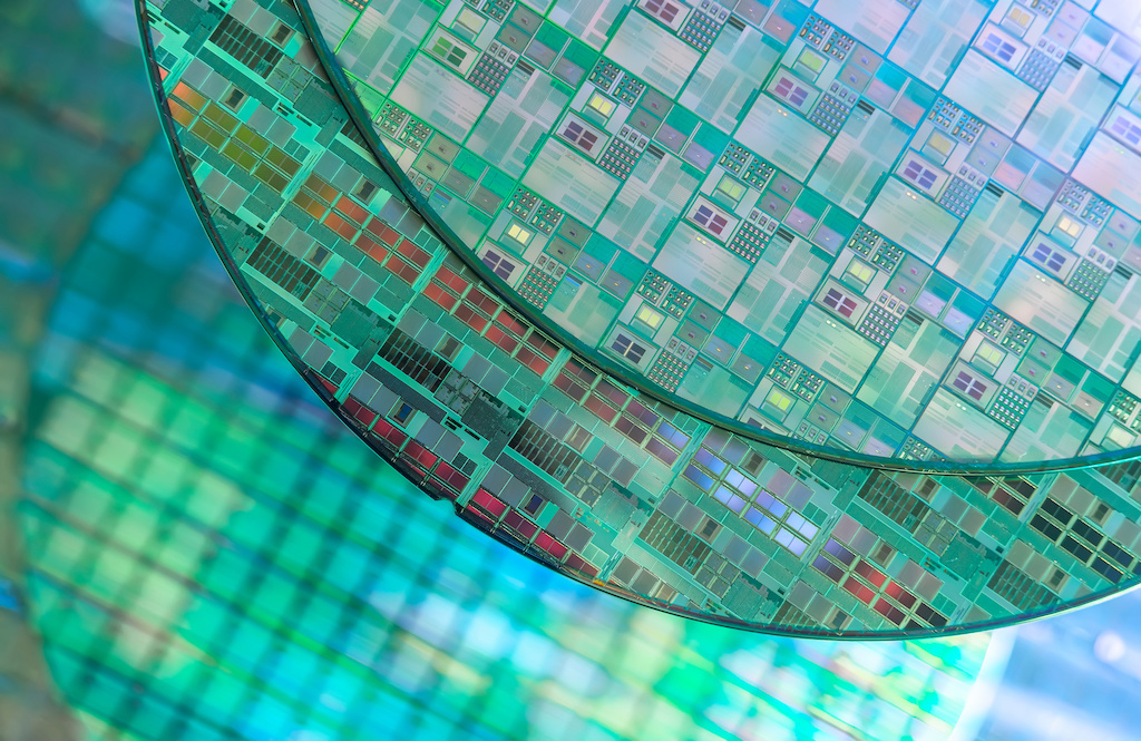
A new technical paper titled “Future of plasma etching for microelectronics: Challenges and opportunities” was published by researchers from numerous academic institutions and companies, including University of Maryland, IBM, Arkema, UCLA, Lam Research, Intel Corporation, Samsung, Air Liquide, Sony, and many others.
Abstract:
“Plasma etching is an essential semiconductor manufacturing technology required to enable the current microelectronics industry. Along with lithographic patterning, thin-film formation methods, and others, plasma etching has dynamically evolved to meet the exponentially growing demands of the microelectronics industry that enables modern society. At this time, plasma etching faces a period of unprecedented changes owing to numerous factors, including aggressive transition to three-dimensional (3D) device architectures, process precision approaching atomic-scale critical dimensions, introduction of new materials, fundamental silicon device limits, and parallel evolution of post-CMOS approaches. The vast growth of the microelectronics industry has emphasized its role in addressing major societal challenges, including questions on the sustainability of the associated energy use, semiconductor manufacturing related emissions of greenhouse gases, and others. The goal of this article is to help both define the challenges for plasma etching and point out effective plasma etching technology options that may play essential roles in defining microelectronics manufacturing in the future. The challenges are accompanied by significant new opportunities, including integrating experiments with various computational approaches such as machine learning/artificial intelligence and progress in computational approaches, including the realization of digital twins of physical etch chambers through hybrid/coupled models. These prospects can enable innovative solutions to problems that were not available during the past 50 years of plasma etch development in the microelectronics industry. To elaborate on these perspectives, the present article brings together the views of various experts on the different topics that will shape plasma etching for microelectronics manufacturing of the future.”
Find the technical paper here. Published June 2024.
Gottlieb S. Oehrlein, Stephan M. Brandstadter, Robert L. Bruce, Jane P. Chang, Jessica C. DeMott, Vincent M. Donnelly, Rémi Dussart, Andreas Fischer, Richard A. Gottscho, Satoshi Hamaguchi, Masanobu Honda, Masaru Hori, Kenji Ishikawa, Steven G. Jaloviar, Keren J. Kanarik, Kazuhiro Karahashi, Akiteru Ko, Hiten Kothari, Nobuyuki Kuboi, Mark J. Kushner, Thorsten Lill, Pingshan Luan, Ali Mesbah, Eric Miller, Shoubhanik Nath, Yoshinobu Ohya, Mitsuhiro Omura, Chanhoon Park, John Poulose, Shahid Rauf, Makoto Sekine, Taylor G. Smith, Nathan Stafford, Theo Standaert, Peter L. G. Ventzek; Future of plasma etching for microelectronics: Challenges and opportunities. J. Vac. Sci. Technol. B 1 July 2024; 42 (4): 041501. https://doi.org/10.1116/6.0003579.
- SEO Powered Content & PR Distribution. Get Amplified Today.
- PlatoData.Network Vertical Generative Ai. Empower Yourself. Access Here.
- PlatoAiStream. Web3 Intelligence. Knowledge Amplified. Access Here.
- PlatoESG. Carbon, CleanTech, Energy, Environment, Solar, Waste Management. Access Here.
- PlatoHealth. Biotech and Clinical Trials Intelligence. Access Here.
- Source: https://semiengineering.com/plasma-etching-challenges-and-options-going-forward-umd-ibm-lam-research-intel-samsung-et-al/

