Physicists have produced an electronic structure known as a flat band in a three-dimensional material for the first time. The flat band was created by trapping an electron within a crystal called a pyrochlore, and an international team led by Joseph Checkelsky and Riccardo Comin of the Massachusetts Institute of Technology (MIT), US, used it to transform the material into a superconductor. As well as superconductivity, the material could offer a platform for studying other physics that arises from strongly correlated electrons, including novel forms of magnetism and electronic symmetry breaking. What is more, the team say the flat-band state could, in principle, appear in other combinations of atoms, provided the atoms occupy an arrangement known as a line graph lattice.
Flat electronic bands are interesting for physicists because electrons become “dispersionless” in these bands – that is, their kinetic energy is completely suppressed so that they can no longer move so freely in a material lattice. As the electrons slow almost to a halt, they become localized at specific positions in the lattice and begin to interact strongly with one other in coordinated ways. This has several physical consequences. Among them is that the electrons’ effective mass approaches infinity, which produces exotic topological phenomena and strongly correlated states of matter associated with high-temperature superconductivity, magnetism and other quantum properties of solids.
Although researchers have created flat-band states in 2D materials before, it has proven difficult to maintain these states in 3D. This is because the electrons that are trapped in 2D “escape” via the third dimension.
Kagome lattices
In a previous study, researchers led by Checkelsky and Comin observed trapped electrons in a 2D kagome lattice – a pattern formed by interconnected, corner-sharing triangles. In this lattice, which is named after a similar structure that appears in traditional Japanese baskets, electrons become confined with the hexagonal space between the triangles. However, while the electrons could not hop across the 2D kagome lattice, they could escape up and out of it.
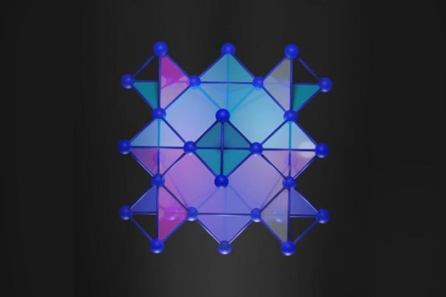
The team has now remedied this by creating a flat-band state in a 3D lattice material, CaNi2. This material, known technically as a C15 Laves phase metal, contains nickel atoms arranged in a pyrochlore, which is a 3D structural arrangement made up of a repeating pattern of cubes. The face of each cube resembles a kagome lattice and electrons become trapped by the geometry of the atomic “scaffolding” surrounding them.
“When the electrons simultaneously try to hop out from this trap, they collide with each other on their way out and their quantum-mechanical trajectories are self-destroying,” Comin explains. “This effect occurs because the electrons can only escape by hopping to a neighbouring atom but the geometrical arrangement of the atoms makes them collide with each other destructively so that they are eventually forced to stay in the trap.”
The same flat band of energy
The researchers confirmed their results by measuring the energy of individual electrons in the crystal to show that they all fell into the same flat band. They did this using a targeted technique called angle-resolved photoemission spectroscopy (ARPES). Here, a single photon of light is focused onto specific locations across the uneven surface of the 3D material. In response, the material emits a single electron, and the energy of this electron can then be precisely measured using a detector. This technique enabled the researchers to “map” the energies of individual electrons across the material’s surface – something that would not be possible with standard photoemission experiments.

Physicists measure electron’s ‘topological spin’
In a further experiment, the team manipulated the correlated electrons by synthesizing the same crystal geometry with atoms of rhodium and ruthenium instead of nickel. They calculated that this structure shifts the electrons’ flat band energy to zero, which leads to superconductivity as electrons pair up.
Comin says the discovery will enable physicists to design and create new classes of quantum materials. “Superconductors are the quintessential quantum materials, where electrons work collectively to realize a quantum ‘choreography’ that translates to various exotic phenomena not displayed by ordinary materials,” he says. As examples, he cites electrical current flow without dissipation (zero resistance); magnetic levitation (perfect diamagnetism, or the Meissner effect) and the realization of quantum devices through quantum interference and the Josephson effect.
The discovery of 3D flat bands also enables a new set of design rules that Comin says will broaden and diversify the playground of quantum solids, including superconductors among other types of materials. The team now plans to study such lattice-born flat bands in other materials.
They report their present work in Nature
- SEO Powered Content & PR Distribution. Get Amplified Today.
- PlatoData.Network Vertical Generative Ai. Empower Yourself. Access Here.
- PlatoAiStream. Web3 Intelligence. Knowledge Amplified. Access Here.
- PlatoESG. Carbon, CleanTech, Energy, Environment, Solar, Waste Management. Access Here.
- PlatoHealth. Biotech and Clinical Trials Intelligence. Access Here.
- Source: https://physicsworld.com/a/crystalline-material-traps-electrons-in-3d/


