| Dec 17, 2023 |
|
|
|
(Nanowerk Spotlight) Scientists have sought to leverage atomic defects to enhance electrocatalytic performance for clean energy applications. However, the inability to precisely study defects’ atomic-scale electric field polarization hindered understanding of the structure-property relationships underlying observed catalytic improvements. Now, new microscopy advances enable direct imaging of electric field distortions in atomic defects, unlocking new design principles.
|
|
Recent innovations in materials defect engineering aim to modulate surface charge distributions and realize property improvements, but lack of characterization techniques created knowledge gaps. Computational predictions indicated defect-induced asymmetric surface charges likely explain enhancements, yet experimental validation remained absent. While introducing defects demonstrably boosted performance, specific defect configurations for optimal effects stayed unclear without fine-scale imaging.
|
|
Advances in aberration-corrected scanning transmission electron microscopy (AC-STEM) overcame previous limits by enabling clear imaging of materials’ atomic structures. Still, tracking electric field distributions surrounding defect sites continued posing difficulties. The newly developed differential phase contrast (DPC) technology within advanced microscopes bridges this gap by sensitively mapping localized electric field distortions.
|
|
DPC’s capacity to reveal nanoscopic environment perturbations around defects showcases its potential to directly relate atomic structures to resultant properties. Recently, a team of researchers in China leveraged DPC to elucidate defect engineering mechanisms for electrocatalytic hydrogen evolution.
|
|
Their research, published in Nature Communications (“Atomic-level polarization in electric fields of defects for electrocatalysis”), acts as demonstration for applying these characterization techniques to directly unravel defect tuning processes across energy domains.
|
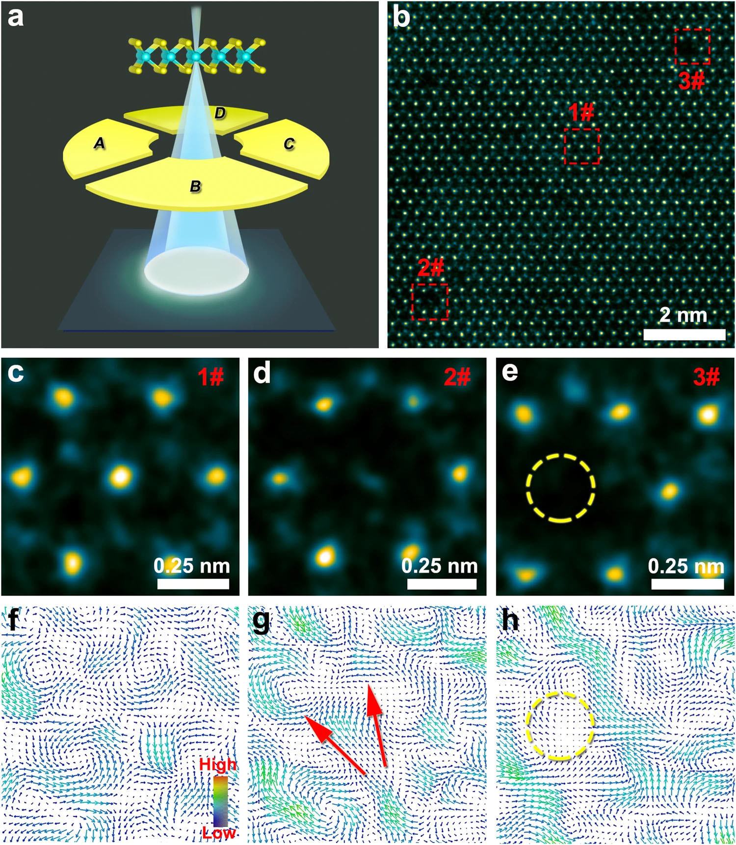 |
| a Imaging mechanism of DPC-STEM. b HAADF-STEM imaging area of S2Mo-MoS2-5 corresponding to the electric field signal collected by the DPC segment detector. c–e Enlarged regions of pristine atomic structure (c), the antisite defect structure (d), and Mo vacancy structure (e), which correspond to the regions of 1#, 2#, and 3# in (b). f–h Atomic electric field distribution images corresponding to (c, d). The directions of the arrows in (f-h) indicate the directions of the electric fields, and the different colors of the arrows indicate the intensities of the electric fields. The red arrows in (g) indicate the electric field polarization region. (Reprinted from doi:0.1038/s41467-023-43689-y under a CC BY 4.0 Deed license)
|
|
Two of the paper’s authors, Yifei Yuan and Jie Xu from Wenzhou University, explain to Nanowerk that, despite years of visualizing atomic defects through electron microscopy, the specific electric fields associated with these defects remain largely unexplored. This lack of understanding creates a significant gap between the mere existence of these defects and their unique catalytic properties. They propose that directly imaging these electric fields could bridge this gap, effectively linking atomic-scale phenomena with the performance of materials at the bulk level.
|
|
Electrocatalytic efficiency constitutes a pivotal factor for many renewable energy devices, making enhancement vital. The researchers targeted defect incorporation within monolayer molybdenum disulfide (MoS2), an earth-abundant electrocatalyst. Introducing sulfur atoms in molybdenum sites (a type of defect known as “antisite”) along with molybdenum vacancy defects into the material’s structure aimed to modulate its electric field distribution and corresponding hydrogen adsorption capability. This process, which involves placing sulfur atoms where molybdenum atoms would typically be, alters the material’s properties for improved performance.
|
|
The team’s chemical vapor deposition approach produced pristine monolayer MoS2 before subjecting samples to controlled annealing under hydrogen/argon flow. This treatment generated specific point defects, confirmed through AC-STEM imaging. The team produced samples with just molybdenum vacancies, samples featuring only antisites, and samples with both defect varieties. Aberration correction enabled clear resolution of individual sulfur atoms occupying vacant molybdenum lattice sites.
|
|
Micro-electrochemical testing revealed over 150 millivolt lower hydrogen evolution reaction overpotential for optimal S2Mo-MoS2 samples containing plentiful antisite defects compared to pristine MoS2. This performance boost indicated substantially improved hydrogen adsorption stemming from the modulated electric field after defect incorporation.
|
|
Elucidating the specific mechanism underlying enhanced electrocatalysis necessitated characterizing defect sites’ atomic-scale environment. The researchers deployed DPC within an advanced STEM to directly visualize electric field distributions surrounding individual atoms. For pristine MoS2, DPC images showed the expected symmetric field. However, antisite defects exhibited pronounced asymmetric polarization, aligning with computational predictions about distorted charge densities.
|
|
Notably, DPC mapping of the same microstructural area eliminated sample-specific differences influencing results. Together with density functional theory calculations, the atomic-scale electric field imaging demonstrated that lowered hydrogen adsorption barriers at polarized antisite defects directly explained the electrocatalytic improvements.
|
|
Beyond elucidating tunable electrocatalysis in this study, the authors underline the potential of directly connecting engineered defects to functional outputs through microscopic electric field characterization. Advances in resolutions and detection modes equip researchers to shift from speculating about proposed defect tuning mechanisms toward directly visualizing local environment variations.
|
|
The team suggests that their approach combining controlled incorporation of specific defect motifs with in situ atomic-scale property characterization lays groundwork for further unraveling structure-property relationships. Tailoring defects while imaging their effects constitutes a promising materials-by-design strategy spanning from catalysis to electronics and energy storage.
|
|
As detection modes continue improving, operando microscopy offers another frontier by enabling real-time monitoring of dynamic processes. Incorporating micro-electrochemical cells into advanced microscopes could reveal electrocatalytic mechanisms fluctuating under operating conditions. This capacity for time-resolved atomic imaging may uncover further surprising environment-property insights.
|
|
Overall, directly quantifying defect engineering outcomes through advanced microscopy lifts assumptions and uncertainties obscuring tunable nanoscale systems’ underlying workings. Rather than relying on inference about hypothesized enhancement factors, researchers can now pinpoint atomic-level causes for emerging behaviors. Defect characterization approaches will likely become ubiquitous as tools probing new structure-property frontiers and accelerating knowledge-driven materials innovation.
|
|

By
Michael
Berger
– Michael is author of three books by the Royal Society of Chemistry:
Nano-Society: Pushing the Boundaries of Technology,
Nanotechnology: The Future is Tiny, and
Nanoengineering: The Skills and Tools Making Technology Invisible
Copyright ©
Nanowerk LLC
|
|
|
- SEO Powered Content & PR Distribution. Get Amplified Today.
- PlatoData.Network Vertical Generative Ai. Empower Yourself. Access Here.
- PlatoAiStream. Web3 Intelligence. Knowledge Amplified. Access Here.
- PlatoESG. Carbon, CleanTech, Energy, Environment, Solar, Waste Management. Access Here.
- PlatoHealth. Biotech and Clinical Trials Intelligence. Access Here.
- Source: https://www.nanowerk.com/spotlight/spotid=64273.php

