| Nov 04, 2023 |
| (Nanowerk News) Two-dimensional (2D) materials – materials just a few atoms thick – can have special properties due to quantum mechanics. What makes these materials special is often their defects. But there are a huge number of potential defects, and they aren’t all useful.
|
|
That makes it challenging for scientists studying these materials. To solve this challenge, researchers developed an automated method to analyze an important part of the 2D materials puzzle – how matter interacts with electromagnetic radiation. The method combines scanning tunneling microscopy (STM) with artificial intelligence (AI) and machine learning (ML).
|
|
This combination results in a quicker and more reliable way to map atomic and electronic features. It allows researchers to examine the range of atomic defects and the electronic fingerprints of materials. It is relatively easy to use even for users who aren’t STM experts.
|
|
The findings have been published in npj Computational Materials (“Autonomous scanning probe microscopy investigations over WS2 and Au{111}”).
|
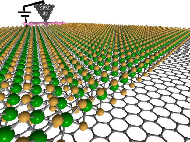 |
| Illustration depicts an autonomous experiment that directs an ultrasharp Scanning Probe Microscopy (SPM) tip across a 2D material surface, capturing the local atomic and electronic structures. (Image: Lawrence Berkeley National Laboratory)
|
|
The new method enables researchers to fully examine 2D surfaces. It offers a means of autonomous experimentation that is fast and accessible. This opens the door to the detailed exploration of novel materials, including quantum materials. The techniques and software could be extended to other techniques in scanning probe microscopy. The researchers have summarized the method in a user-friendly, open access, and tailorable software package.
|
|
Two-dimensional material systems are much sought after due to the enormous functional phase space spanning from insulating to conducting properties, which is driven by atomic-scale and nanoscale defects that can be tuned by layer thickness, heterostructure stacking, twisting, and other methods. Techniques that provide spectroscopic insight, such as STM, are extremely important for researchers correlating nano defective states with macroscopic properties.
|
|
However, while hyperspectral scanning tunneling spectroscopy imaging provides critical insight into heterogenous electronic properties at the atomic scale, its analysis is impeded by the enormous time required. For instance, a hyperspectral optical map collected at 10 minutes per point in a 150 by 150-pixel grid would take well over one month to analyze.
|
|
The research team at Lawrence Berkeley National Laboratory’s Molecular Foundry, a Department of Energy Office of Science user facility, developed a means of performing spatially dense, point spectroscopic measurements with an STM in combination with AI and ML. This approach provides faster and more accurate statistically averaged data that map and identify spectroscopic signatures of heterogeneous surfaces.
|
|
Using tungsten disulfide (WS2) and gold (Au-111) surfaces as a benchmark, the team demonstrated how to perform measurements with reproducible resulting spectra and how to create statistically significant electronic structure characterization of the different intrinsic defects that can be found on samples of interest.
|
- SEO Powered Content & PR Distribution. Get Amplified Today.
- PlatoData.Network Vertical Generative Ai. Empower Yourself. Access Here.
- PlatoAiStream. Web3 Intelligence. Knowledge Amplified. Access Here.
- PlatoESG. Carbon, CleanTech, Energy, Environment, Solar, Waste Management. Access Here.
- PlatoHealth. Biotech and Clinical Trials Intelligence. Access Here.
- Source: https://www.nanowerk.com/nanotechnology-news2/newsid=63999.php

