Home > Press > Wafer-scale 2D MoTe₂ layers enable highly-sensitive broadband integrated infrared detector
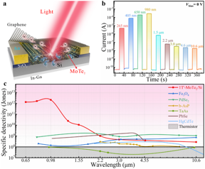 |
| a, Schematic illustration of a graphene/1Tʹ-MoTe₂/Si Schottky junction device. b,Time-dependent photoresponse properties to pulsed light illumination in a broad spectral band. c, Comparison of the room-temperature specific detectivity of the Gr/1Tʹ-MoTe₂/Si Schottky junction device with other devices. CREDIT by Di Wu, Chenguang Guo, Longhui Zeng, Xiaoyan Ren, Zhifeng Shi, Long Wen, Qin Chen, Meng Zhang, Xin Jian Li, Chong-Xin Shan, and Jiansheng Jie |
Abstract:
Detection in multiple infrared (IR) regions spanning from short- and mid- to long-wave IR plays an important role in diverse fields from scientific research to wide-ranging technological applications including target identification, imaging, remote monitoring, and gas sensing. Currently, the state-of-the-art IR photodetectors are mainly dominated by conventional narrow bandgap semiconductors including In1-xGaxAs, InSb, and Hg1-xCdxTe, operating in short-wave IR (SWIR, 1-3 µm), mid-wave IR (MWIR, 3-6 µm), and long-wave IR (LWIR, 6-15 µm) spectral bands, respectively. Notably, these photodetectors not only rely on high-temperature growth process of raw materials and complex processing technique, but also suffer from the cryogenic cooling conditions with time-consuming and high power consumption. Moreover, there are several remaining technological challenges such as poor complementary metal-oxide-semiconductor (CMOS) compatibility, bulky module size, and low efficiency, which severely restrict the wider application of these detectors.
Wafer-scale 2D MoTe₂ layers enable highly-sensitive broadband integrated infrared detector
Changchun, China | Posted on January 6th, 2023
In a new paper published in Light Science & Application, Prof. Di Wu and Xinjian Li from Zhengzhou University, Dr. Longhui Zeng from the University of California-San Diego, and Prof. Jiansheng Jie from Soochow University demonstrated a facile thermal-assisted tellurization route for the van der Waals (vdW) growth of wafer-scale phase-controlled 2D MoTe2 layers. The type-II Weyl semimetal 1T′-MoTe2 layers were directly deposited on prepatterned Si substrate to in-situ fabricate 1T’-MoTe2/Si vertical Schottky junction. The high-quality Schottky junction interface and vertical device structure with graphene electrode ensure efficient carrier transport and reduce carrier recombination, enabling the detector to achieve an ultrabroadband detection range of up to 10.6 μm and a room-temperature specific detectivity of over 108 Jones in the mid-infrared region. The wafer-scale 2D MoTe2 layers have also enabled the integrated device array to be successfully implemented for high-resolution uncooled mid-infrared imaging.
In this study, a pre-deposited Mo film as a precursor was transformed to 2D MoTe2 layer via vdW growth mechanism through a direct thermal-assisted tellurization process. As a matter of fact, the phase transition of MoTe2 is highly dependent on the growth time. By controlling the growth time, 2-inch 2H and 1Tʹ- MoTe2 layers with good uniformity were obtained, respectively. By virtue of the facile and scalable thermal-assisted tellurization strategy, the thickness of the 2D MoTe2 layers can be precisely tailored by tuning the initial Mo film thickness.
The vdW growth of the large-area 2D MoTe2 layers offers more flexibility for the development of high-sensitivity optoelectrical devices. In light of this, a 1Tʹ-MoTe2/Si vertical Schottky junction device was developed by the in-situ vdW growth of 1Tʹ-MoTe2 layers on a pre-patterned Si substrate. To ensure the efficient carrier collection, monolayer graphene was selected as a top transparent contact with 1Tʹ-MoTe2 layer. The photodetector demonstrates high-sensitive self-powered ultrabroadband detection performance with a detection range of up to 10.6 µm and a large room-temperature specific detectivity of over 108 Jones in the mid-infrared (MIR) range. The obtained room-temperature specific detectivity is superior to the most 2D material-based IR detectors and some commercial detectors.
Given the superior IR detection capability of the photodetector, the room-temperature IR imaging was further explored with the Gr/1Tʹ-MoTe2/Si Schottky junction device. The photocurrent mapping image of “LWIR” pattern with a large current contrast ratio over 10 and sharp edges was obtained from an individual detector under the IR illumination of 10.6 μm at room temperature. Furthermore, the large-scale uniform 2D MoTe2 layer enables the fabrication of an 8 × 8 1Tʹ-MoTe2/Si Schottky junction device array for IR imaging application. Upon MIR laser illumination, the large difference between the currents of the exposed and unexposed pixels results in a high-resolution heart-shaped image with large current ratios of 100, 68, and 51 for 3.0, 4.6, and 10.6 μm laser illumination at room-temperature, respectively. Such excellent room-temperature imaging capability with good homogeneity of the device array makes this finding great promise for MIR imaging applications. The wafer-scale growth of 2D MoTe2 layers compatible with Si technology shows great potential for next-generation on-chip Si CMOS systems with low-power consumption and low-cost production.
####
For more information, please click here
Contacts:
Media Contact
Yaobiao Li
Light Publishing Center, Changchun Institute of Optics, Fine Mechanics And Physics, CAS
Office: 86-431-861-76851
Expert Contact
Xinjian Li
Zhengzhou University, China
Copyright © Light Publishing Center, Changchun Institute of Optics, Fine Mechanics And Physics, CAS
If you have a comment, please Contact us.
Issuers of news releases, not 7th Wave, Inc. or Nanotechnology Now, are solely responsible for the accuracy of the content.
Bookmark:


| Related Links |
| Related News Press |
News and information
![]() Electricity harvesting from evaporation, raindrops and moisture inspired by nature January 6th, 2023
Electricity harvesting from evaporation, raindrops and moisture inspired by nature January 6th, 2023
![]() Lithium-sulfur batteries are one step closer to powering the future January 6th, 2023
Lithium-sulfur batteries are one step closer to powering the future January 6th, 2023
2 Dimensional Materials
![]() Team undertakes study of two-dimensional transition metal chalcogenides Important biomedical application, including biosensing December 9th, 2022
Team undertakes study of two-dimensional transition metal chalcogenides Important biomedical application, including biosensing December 9th, 2022
Imaging
![]() Shrinking hydrogels enlarge nanofabrication options: Researchers from Pittsburgh and Hong Kong print intricate, 2D and 3D patterns December 29th, 2022
Shrinking hydrogels enlarge nanofabrication options: Researchers from Pittsburgh and Hong Kong print intricate, 2D and 3D patterns December 29th, 2022
![]() New X-ray imaging technique to study the transient phases of quantum materials December 29th, 2022
New X-ray imaging technique to study the transient phases of quantum materials December 29th, 2022
![]() Rapid fluorescent mapping of electrochemically induced local pH changes December 9th, 2022
Rapid fluorescent mapping of electrochemically induced local pH changes December 9th, 2022
Possible Futures
![]() Development of bio-friendly transparent temperature sensor technology that precisely measures temperature changes by light January 6th, 2023
Development of bio-friendly transparent temperature sensor technology that precisely measures temperature changes by light January 6th, 2023
![]() Dual-site collaboration boosts electrochemical nitrogen reduction on Ru-S-C single-atom catalyst January 6th, 2023
Dual-site collaboration boosts electrochemical nitrogen reduction on Ru-S-C single-atom catalyst January 6th, 2023
Chip Technology
![]() New X-ray imaging technique to study the transient phases of quantum materials December 29th, 2022
New X-ray imaging technique to study the transient phases of quantum materials December 29th, 2022
![]() Experimental nanosheet material marks a step toward the next generation of low-power, high-performance electronics December 9th, 2022
Experimental nanosheet material marks a step toward the next generation of low-power, high-performance electronics December 9th, 2022
![]() Tin selenide nanosheets enables to develop wearable tracking devices December 9th, 2022
Tin selenide nanosheets enables to develop wearable tracking devices December 9th, 2022
Sensors
![]() Development of bio-friendly transparent temperature sensor technology that precisely measures temperature changes by light January 6th, 2023
Development of bio-friendly transparent temperature sensor technology that precisely measures temperature changes by light January 6th, 2023
![]() New nanowire sensors are the next step in the Internet of Things January 6th, 2023
New nanowire sensors are the next step in the Internet of Things January 6th, 2023
![]() Tin selenide nanosheets enables to develop wearable tracking devices December 9th, 2022
Tin selenide nanosheets enables to develop wearable tracking devices December 9th, 2022
Discoveries
![]() Electricity harvesting from evaporation, raindrops and moisture inspired by nature January 6th, 2023
Electricity harvesting from evaporation, raindrops and moisture inspired by nature January 6th, 2023
![]() Lithium-sulfur batteries are one step closer to powering the future January 6th, 2023
Lithium-sulfur batteries are one step closer to powering the future January 6th, 2023
![]() New nanowire sensors are the next step in the Internet of Things January 6th, 2023
New nanowire sensors are the next step in the Internet of Things January 6th, 2023
Announcements
![]() Electricity harvesting from evaporation, raindrops and moisture inspired by nature January 6th, 2023
Electricity harvesting from evaporation, raindrops and moisture inspired by nature January 6th, 2023
![]() Lithium-sulfur batteries are one step closer to powering the future January 6th, 2023
Lithium-sulfur batteries are one step closer to powering the future January 6th, 2023
![]() New nanowire sensors are the next step in the Internet of Things January 6th, 2023
New nanowire sensors are the next step in the Internet of Things January 6th, 2023
Interviews/Book Reviews/Essays/Reports/Podcasts/Journals/White papers/Posters
![]() Electricity harvesting from evaporation, raindrops and moisture inspired by nature January 6th, 2023
Electricity harvesting from evaporation, raindrops and moisture inspired by nature January 6th, 2023
![]() Lithium-sulfur batteries are one step closer to powering the future January 6th, 2023
Lithium-sulfur batteries are one step closer to powering the future January 6th, 2023
![]() New nanowire sensors are the next step in the Internet of Things January 6th, 2023
New nanowire sensors are the next step in the Internet of Things January 6th, 2023
- SEO Powered Content & PR Distribution. Get Amplified Today.
- Platoblockchain. Web3 Metaverse Intelligence. Knowledge Amplified. Access Here.
- Source: http://www.nanotech-now.com/news.cgi?story_id=57267

