News: Microelectronics
26 October 2023
A consortium led by the University of Vermont (UVM) — and including GlobalFoundries, the Vermont Agency of Commerce and Community Development, and the Vermont State College System — has been designated as one of 31 Tech Hubs by the US Department of Commerce’s Economic Development Administration (EDA), unlocking the opportunity for up to $75m in federal grant funding to further research in semiconductor technology.
‘Advancing Gallium Nitride (GaN) Technology in the Greater Burlington Area’ was selected by the Tech Hubs program from nearly 400 applications. The aim of the program is to “strengthen US economic and national security by catalyzing technology-based regional growth that enables the industries of the future to start, grow and remain in regions across our country,” according to the EDA’s announcement of the designation, which corresponded with a live event hosted by President Biden on 23 October.
The EDA designation paves the way for the consortium to apply for Phase II of the program, which will culminate in award implementation grants totaling $50–75m to each of 5–10 Tech Hubs.
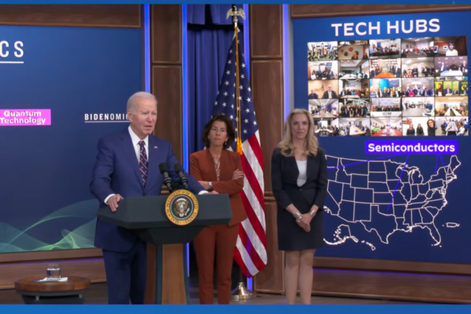
Picture: US President Joe Biden, joined by Secretary of Commerce Gina Raimondo and Director of the National Economic Council Lael Brainard, announces the Tech Hubs program at the Eisenhower Executive Office Building on 23 October.
“Investment in American innovation and supply chain independence is essential to our nation’s economic security and global competitiveness. We appreciate the Biden Administration and Congress for investing in this area, and the EDA for recognizing the important role small, more rural states like Vermont will have,” said Governor Phil Scott.
The goal of the Vermont Tech Hub is to build and sustain a successful ecosystem for advancing GaN and other semiconductor innovations and, in the process, to grow the economy and economic vitality of the region and the state.
“GlobalFoundries looks forward to deepening our partnership with UVM, working together to realize the full potential of high-volume manufacturing of GaN on silicon chips, and to driving US leadership in this emerging technology,” says Ken McAvey, VP & general manager of GlobalFoundries Vermont. “The CHIPS and Science Act has proven to be a successful catalyst for renewed enthusiasm, collaboration and investment in US semiconductor manufacturing, and the Tech Program will be a critical vehicle for advancing new technologies through development and into the marketplace.”
The estimated global demand for GaN and related semiconductor solutions is growing, and the technology invites significant potential uses and offers advantages over existing semiconductor technology — adding speed, power and efficiency. GaN has the potential for many applications, including high-frequency radio communications, power electronics, automotive electronics, aerospace applications, high-performance medical imaging equipment, and consumer electronics.
“EDA Tech Hub designation is an important step in our plan to build a successful innovation economy for Vermont — in the area of semiconductor materials and advanced chip design,” says Kirk Dombrowski, UVM vice president for Research and Economic Development.
Signed into law in August 2022, the CHIPS and Science Act authorized $10bn in funding for the Tech Hubs Program. EDA has received $500m (5%) of the authorized dollar amount and has designated 31 Tech Hubs and awarded 29 Strategy Development Grants.
At its core, the Tech Hubs Program is an economic development initiative designed to drive technology- and innovation-centric growth by strengthening a region’s capacity to manufacture, commercialize and deploy critical technologies. The consortium’s regional vision is focused on the tech ecosystem that will emerge with the next generation of high-power, high-speed chips based on GaN. The northeast region has the partnerships, technology leaders, and research capacity to become a global leader in this technology, it is reckoned.
The Tech Hub designation follows a week after the launch of UVM’s new Device Characterization Lab, a partnership with GlobalFoundries with funding from the US Department of Education aimed at driving semiconductor research and preparing students for key roles within the field.
GlobalFoundries gains $35m US Government funding to accelerate 200mm GaN-on-Si chip production
GlobalFoundries awarded $30m in US funding for development and production of GaN-on-Si
IQE forms strategic partnership with GlobalFoundries
- SEO Powered Content & PR Distribution. Get Amplified Today.
- PlatoData.Network Vertical Generative Ai. Empower Yourself. Access Here.
- PlatoAiStream. Web3 Intelligence. Knowledge Amplified. Access Here.
- PlatoESG. Carbon, CleanTech, Energy, Environment, Solar, Waste Management. Access Here.
- PlatoHealth. Biotech and Clinical Trials Intelligence. Access Here.
- Source: https://www.semiconductor-today.com/news_items/2023/oct/vermont-gf-261023.shtml

