News: Suppliers
12 July 2023
Taiyo Nippon Sanso Corp (TNSC) of Tokyo, Japan has launched the UR26K-CCD metal-organic chemical vapor deposition (MOCVD) system for the mass production of gallium nitride (GaN).
As its flagship production-scale MOCVD model, with fully automated handling of wafers and parts cleaning, it is reckoned that the UR26K-CCD can increase production efficiency by about 2x compared with conventional systems.

Picture: Taiyo Nippon Sanso’s new UR26K-CCD MOCVD system.
Compared with the existing UR26K commercial production GaN MOCVD system, to boost productivity the new UR26K-CCD is an improved model offering an upgraded ‘Cassette-to-Cassette Wafer Handling System’ automated transfer mechanism and an ‘Integrated Dry-Cleaning System’ for dry-cleaning reactor parts.
These features allow fully automated transfer of wafers inside the unit. Additionally, since the used parts inside the reactor are transferred within the system by the transfer robot to the separately installed dry-cleaning chamber and returned to the reactor after cleaning, the entire epitaxial growth process is handled with clean parts. This automated cycle eliminates the need to interrupt the operation of the growth chamber for the cleaning process, which increases production efficiency by about 2x compared with conventional system.
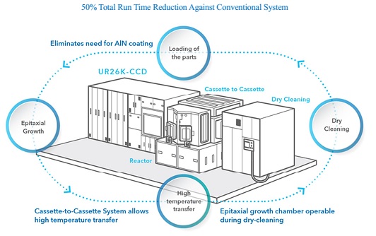
Growing GaN-on-silicon wafers can pose significant challenges to achieving reproducible results, a difficulty attributed to the contamination of wafers due to foreign material and wafer warping. Integrating the cleaning unit and maintaining the consistency of the reactor environment should result in improved reproducibility and higher yield ratios, i.e. lower total cost of ownership, says Taiyo Nippon Sanso.
Accommodating 10×6” or 6×8” wafer sizes, the reactor configuration (face up, rotation & revolution) is the same as the conventional UR26K, which employs the firm’s proprietary three laminar flow horizontal gas nozzles, gear-driven wafer rotation mechanism, and a 6-zone resistance heater for uniform film growth. Sources include TMGa, TEGa, TMAl, TMIn, NH3, Cp2Mg, and SiH4. The growth pressure is 13-100kPa. Applications include power devices, high-frequency devices, and micro-LEDs.
Nippon Sanso and NCSU collaborating on GaN epitaxy and device technology
- SEO Powered Content & PR Distribution. Get Amplified Today.
- PlatoData.Network Vertical Generative Ai. Empower Yourself. Access Here.
- PlatoAiStream. Web3 Intelligence. Knowledge Amplified. Access Here.
- PlatoESG. Automotive / EVs, Carbon, CleanTech, Energy, Environment, Solar, Waste Management. Access Here.
- BlockOffsets. Modernizing Environmental Offset Ownership. Access Here.
- Source: https://www.semiconductor-today.com/news_items/2023/jul/taiyo-nippon-sanso-120723.shtml

