| Mar 22, 2024 |
|
(Nanowerk News) Metal halide perovskites have become well-deserved “star” materials among a variety of semiconductors owing to their excellent optoelectronics properties, such as high photoluminescence (PL) quantum yield (QY), high absorption coefficient, tunable bandgaps, long carrier diffusion lengths, and high defect tolerance, attracting enormous attention from both academia and industry.
|
|
Meanwhile, DLW, based on the interaction between light and matter, is an efficient, contactless, mask free, and depth-resolved micro-patterning technique. It is typically performed by coupling a laser beam with a high-resolution microscope to minimize the output focal spot. The resolution of DLW is dependent on the diameter of the output focal spot and the threshold response of the material.
|
|
Depending on the fabrication mechanisms and material threshold responses, the best resolution is usually between a couple to a few hundreds of nanometers. The research on DLW also deepens the fundamental understanding on the interaction mechanisms between light and perovskites, paving the way for designing optoelectronic devices with improved performances.
|
|
In a review paper published in Light Advanced & Manufacturing (“Direct laser writing on halide perovskites: from mechanisms to applications”), a team of scientists, led by Professor Zhixing Gan from Center for Future Optoelectronic Functional Materials, Nanjing Normal University, China, and co-workers have summarized recent research progress of DLW on perovskites.
|
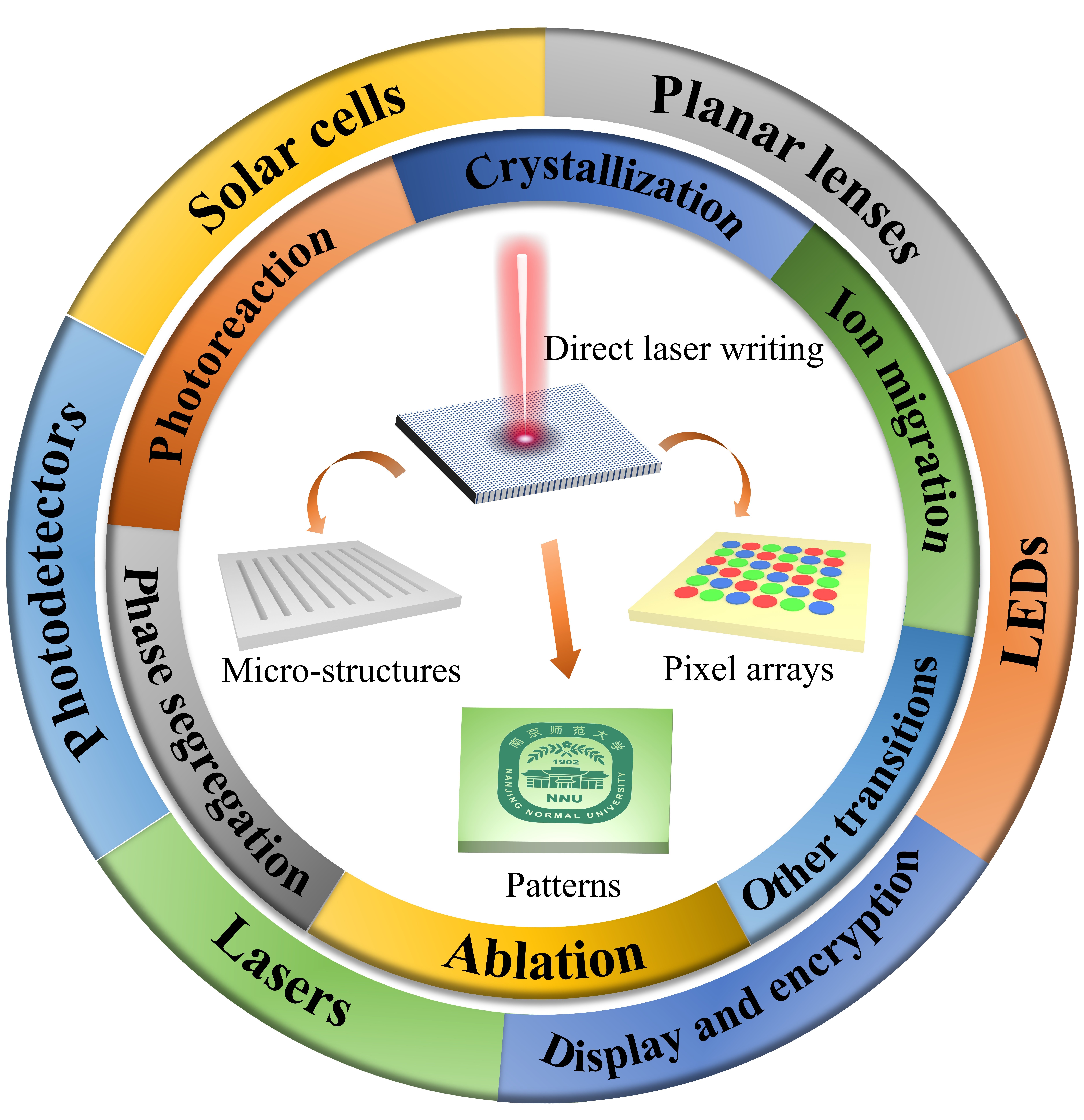 |
| Schematic overview of direct laser writing on halide perovskites: from mechanisms to applications. (Image: Light Advanced & Manufacturing)
|
|
The concrete interaction mechanisms between laser and perovskite are categorized into six parts, including laser ablation, laser induced crystallization, laser induced ion migration, laser induced phase segregation, laser induced photoreaction, and other laser induced transitions. Then, they focus on the applications of these perovskites with micro/nano patterns and array structures, such as display, optical information encryption, solar cells, LEDs, laser, photodetectors, and planar lenses. The advantages of the patterned structures are highlighted. Finally, current challenges for DLW on perovskites are outlooked and perspectives on their future developments are also put forward.
|
|
Laser is an excellent tool to manipulate, fabricate and process nano-/micro-structures on semiconductors with unique advantages of high precision, contactless, easy operation, mask free. DLW based on different interaction mechanisms between laser and perovskites have been developed due to the special structure of perovskites. The detailed interaction mechanism sensitively depends on laser, such as wavelength, pulse/CW, power, and repetition rate, therefore providing a flexible and powerful tool to process the perovskites with precisely controlled nano- or micro-structures. The wide variety of interaction mechanisms determine the DLW’s great potential for various applications in microelectronics, photonics and optoelectronics.
|
|
Cheaper and flexibly controllable fabrication lasers, together with perovskite’s superior optoelectronic properties will bring great application potential for DLW on perovskites. Currently it is still in the infancy stage, anticipating a huge boom in both fundamental research and industry demand in the near future. For the future development of DLW on perovskites, some crucial technical bottlenecks need to be solved, such as the resolution of DLW technique, the existing time of segregated phases, and the micropatterning technique to flexible substrates, etc.
|
|
The applications of perovskites almost cover all sorts of optoelectronic and photonic areas, such as single photon source, micro/nano lasers, photo-detectors, optical gates, optical communication, waveguide, and nonlinear optics. Thus, it is very promising to construct and integrate photonic devices with different functions based on a single perovskite chip.
|
- SEO Powered Content & PR Distribution. Get Amplified Today.
- PlatoData.Network Vertical Generative Ai. Empower Yourself. Access Here.
- PlatoAiStream. Web3 Intelligence. Knowledge Amplified. Access Here.
- PlatoESG. Carbon, CleanTech, Energy, Environment, Solar, Waste Management. Access Here.
- PlatoHealth. Biotech and Clinical Trials Intelligence. Access Here.
- Source: https://www.nanowerk.com/nanotechnology-news3/newsid=64905.php

