| Oct 30, 2023 |
| (Nanowerk News) The diamond in an engagement ring, the wonder-material graphene and the ‘lead’ in a humble pencil are all formed from carbon, but display profoundly different characteristics. Carbon materials such as these are among the most famous examples of how diverse properties can emerge in materials, based only on the rearrangement of the structure of atoms.
|
|
The goal of the RIKEN Center for Emergent Matter Science (CEMS) in Saitama, Japan, is to develop materials for new, energy-efficient technologies. The usual approach to synthesizing new materials involves looking for improved properties such as strength and durability, or enhanced conduction of electricity and heat. But CEMS is pioneering an alternative approach that turns that standard approach on its head. First, we think of the properties needed for a new device, use data from RIKEN’s new repository and simulation platform to calculate the atomic structure that provides these features and then build the bespoke material.
|
Sustainably small
|
|
CEMS is working to shrink electronics, but engineers are hitting many limits in size reduction. For example, you might look at an ‘inductor’, a standard component found in devices such as smart phones. These coils of wire control the flow of electrical current in a circuit by storing it as magnetic field energy.
|
|
At first glance, physicists might assume that the inductor can be made smaller by reducing the size of the coil, but this decreases its ability to store energy.
|
|
A few years ago, physicists at CEMS hit upon an innovative solution. They realized that a peculiar property of certain exotic magnetic materials could mimic an inductor, without needing a wire.1 The feature relates to a quantum characteristic inherent to all electrons called ‘spin’, which turns electrons on an invisible axis that points in a specific direction.
|
|
In normal magnets, the spins of electrons align in one direction, creating the magnetic effect. But the CEMS physicists were intrigued by helimagnets, a set of naturally occurring materials in which the electrons arrange themselves into spirals.
|
|
They thought some electrically-conducting helimagnets could mimic a coil of wire, serving as a tiny inductor: that notion was borne out in CEMS experiments in 2020 (Nature, “Emergent electromagnetic induction in a helical-spin magnet”).
|
|
While the first helimagnets investigated operated only at energy intensive ultra-cold temperatures, CEMS researchers found one that works at room temperature, in collaboration with the University of Tokyo (PNAS, “Emergent electromagnetic induction beyond room temperature”).
|
|
There are, however, other obstacles to overcome. For example, helimagnets only work below the megahertz regime, but devices such as a cellphones operate at frequencies in the much higher gigahertz range.
|
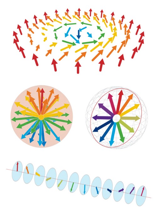 |
| Helimagnets are a set of naturally occurring materials in which the electrons arrange themselves into spirals. Some tiny electrically-conducting helimagnets could mimic an inductor—coils of wire that control the flow of electrical current in a circuit by storing it as magnetic field energy. (Image: RIKEN)
|
Magnetic memory
|
|
Another tiny, twisting technology being investigated at CEMS could help revolutionize memory storage in electronics.
|
|
It involves skyrmions—spherical knots of electrons oriented so that their spins all point outwards, a bit like a curled-up hedgehog. These configurations are very stable because they only unfurl when extra energy is put into the system.
|
|
Skyrmions act like particles because they are easy to move around with an external magnetic field and are difficult to destroy. This makes them an attractive tool for storing information, which would be encoded in the position of the skyrmion. Since they are so stable, they are also robust against errors and memory corruption.
|
|
Crucially, they are also minuscule: a skyrmion can be smaller than one hundredth of a micrometer, which means you can pack 10,000 skyrmions into just 1 μm2 (micrometer squared), which is one tenth to one hundredth the width of a human hair.
|
|
This would enable very high-density memory storage and smaller memory storage devices.
|
|
But, once again, there is a stumbling block. So far, physicists have been able to easily manipulate skyrmions in materials with lower densities of the electron knots, but not in the high-density knots they are most interested in.
|
|
A major frustration is that there is no real strategy behind finding the right skyrmion-hosting material. The present approach is to make a compound, measure it, see if it fits and make another compound if it doesn’t.
|
|
Typically, it is chemists who discover new materials, by tweaking the structures of familiar materials. Physicists then catalog any new properties that emerge from them, by meticulously measuring their optical, electrical, magnetic, thermal and mechanical characteristics. Finally, engineers take a material that has useful features and build a device to capitalize on them. It’s all trial-and-error.
|
|
Worse still, scientists only tend to report successful attempts to their peers. This means a lot of time and resources are wasted by different groups repeating the same mistakes.
|
|
CEMS is setting up a new digital platform to make this process more efficient by systematically combining data from lab experiments with supercomputer simulations via an online platform that can be accessed from within RIKEN (see box: A TRIP into the future of material science). The aim is to make it easier for scientists to start with a vision of the device they need and work backwards to create the bespoke material that matches their requirements.
|
A TRIP into the future of material science
|
|
There are only 80 or so kinds of elements that humans can play with in the lab when trying to engineer novel components for devices. But the atoms of these 80 elements can be rearranged to design an almost infinite number of new materials, and this means that studying this involves mind-blowing amounts of data.
|
|
With this in mind, RIKEN’s Center for Emergent Matter Science (CEMS) is contributing to the promotion of ‘TRIP’, or ‘Transformative Research Innovation Platform of RIKEN Platforms,’ a RIKEN-wide initiative aimed at linking the various data platforms within RIKEN to develop new scientific paradigms. CEMS is participating in the initiative through a repository that combines knowledge gained from real-lab experiments with simulations of predicted material properties made by supercomputers. Artificial intelligence, or AI, can then be harnessed to help design useful new materials based on the properties that are wanted, which scientists can then synthesize.
|
|
Takahisa Arima, deputy director of CEMS, says that despite being based in physics, the project takes inspiration from biology, where AI has shown considerable success in recent years at correctly predicting how proteins will fold—once one of the biggest outstanding problems for biologists. “But the challenge for material science is far harder because there are many more building blocks,” says Arima.
|
|
Looking toward the future, TRIP aims to include simulations and predictions made by quantum computers—machines being developed that have the potential to outperform today’s supercomputers—to tackle these problems. “We are pioneering the digital transformation of science,” says Arima.
|
|
Growing up, Arima had a very different ambition. “I wanted to become a meteorologist and forecast the weather. But I changed my mind at university, when I realized just how many complex factors come into play when trying to predict – let alone manipulate – the route of a typhoon, say,” he says.
|
|
“By contrast, condensed matter physics offers an enticing clarity and control. Material properties are very diverse, but they are generated by simple behaviors of electrons and nuclei in atoms.” This combined with increasing computing power, he says, means that materials should have the power to transform our lives sooner than we may think.
|
- SEO Powered Content & PR Distribution. Get Amplified Today.
- PlatoData.Network Vertical Generative Ai. Empower Yourself. Access Here.
- PlatoAiStream. Web3 Intelligence. Knowledge Amplified. Access Here.
- PlatoESG. Carbon, CleanTech, Energy, Environment, Solar, Waste Management. Access Here.
- PlatoHealth. Biotech and Clinical Trials Intelligence. Access Here.
- Source: https://www.nanowerk.com/nanotechnology-news2/newsid=63959.php

