This was the 12th TSMC OIP and it did not disappoint. The attendance was back to pre pandemic levels, there was interesting news and great presentations. We will cover the presentations in more depth after the virtual event which is on November 10th. You can register HERE.
As I mentioned in my previous post, the Jim Keller Keynote would be worth the price of admission and it was. When I first talked about chiplets I sarcastically said that “chiplets are cheating”. We have spent our entire careers figuring out how to design and manufacture complex monolithic chips and now you can go to Chip Depo and get chiplets, open source software, IP, and even AI tools to more easily design complex chips.
Jim Keller is now the president and CTO of Torrent, an AI chip start up, and that is exactly what he is doing. In his keynote Jim talks about 10 problems to solve during this journey to silicon. Don’t miss it.
Here are my key takeaways from the event:
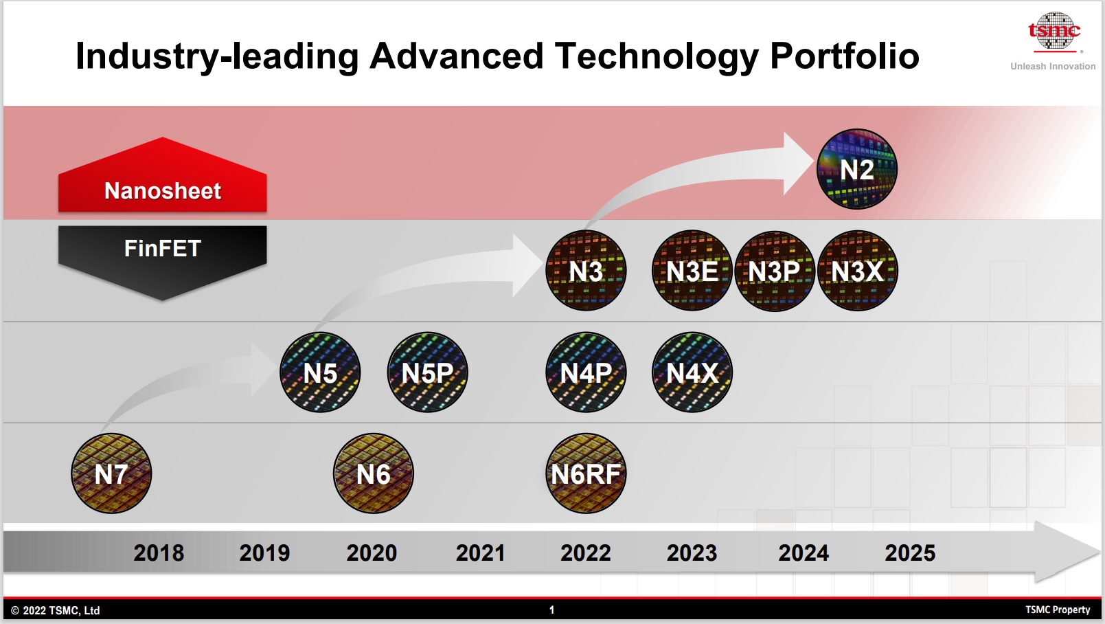
Contrary to what you may have read from the semiconductor outsider media, TSMC’s progress with advanced nodes is going as planned. N3 wafers are shipping to Apple, N3E, N4X, N3P, N3X, and N2 are on track.
Remember, N3 is Apple SoC specific. N3E is an enhanced version for the masses: Intel, AMD, NVIDIA, Qualcomm, etc… Over the next two years we will see more N3 tape-outs than any prior FinFET node, absolutely.

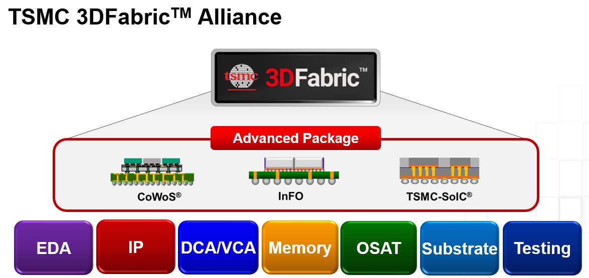
TSMC also expanded the OIP ecosystem to include a 3D Fabric Alliance. As I have mentioned many times semiconductors is all about the ecosystem and you will never see a more powerful ecosystem in the semiconductor industry or any other industry for that matter.
According to L.C. Lu, TSMC fellow and vice president of design and technology platform, more than 3,000 TSMC employees are part of OIP plus 10,000 people from the more than 100 OIP partners. The OIP now includes 50,000 titles, 43,000 tech files, and 2,800 PDKs.
This new alliance strengthens TSMC’s leadership in the chip packaging business. The press release provides nice detail on the new alliance but here are some clips:

The new TSMC 3DFabric™ Alliance is TSMC’s sixth OIP Alliance and the first of its kind in the semiconductor industry that joins forces with partners to accelerate 3D IC ecosystem innovation and readiness, with a full spectrum of best-in-class solutions and services for semiconductor design, memory modules, substrate technology, testing, manufacturing, and packaging. This alliance will help customers achieve speedy implementation of silicon and system-level innovations and enable next-generation HPC and mobile applications using TSMC’s 3DFabric technologies, a comprehensive family of 3D silicon stacking and advanced packaging technologies.
“3D silicon stacking and advanced packaging technologies open the door to a new era of chip-level and system-level innovation, and also require extensive ecosystem collaboration to help designers navigate the best path through the myriad options and approaches available to them,” said Dr. L.C. Lu, TSMC fellow and vice president of design and technology platform. “Through the collective leadership of TSMC and our ecosystem partners, our 3DFabric Alliance offers customers an easy and flexible way to unlocking the power of 3D IC in their designs, and we can’t wait to see the innovations they can create with our 3DFabric technologies.”
OIP 3DFabric Alliance
As the industry’s most comprehensive and vibrant ecosystem, the TSMC OIP consists of six alliances: the EDA Alliance, IP Alliance, Design Center Alliance (DCA), Value Chain Alliance (VCA), Cloud Alliance, and now, the 3DFabric Alliance. TSMC launched OIP in 2008 to help customers overcome the rising challenges of semiconductor design complexity by creating a new paradigm of collaboration, organizing development and optimization across TSMC’s technologies, electronic design automation (EDA), IP, and design methodology.
Partners of the new 3DFabric Alliance have early access to TSMC’s 3DFabric technologies, enabling them to develop and optimize their solutions in parallel with TSMC. This gives customers a head start on their product development with early availability of the highest-quality, readily-available solutions and services from EDA and IP to DCA/VCA, Memory, OSAT (Outsourced Semiconductor Assembly and Test), Substrate, and Testing.
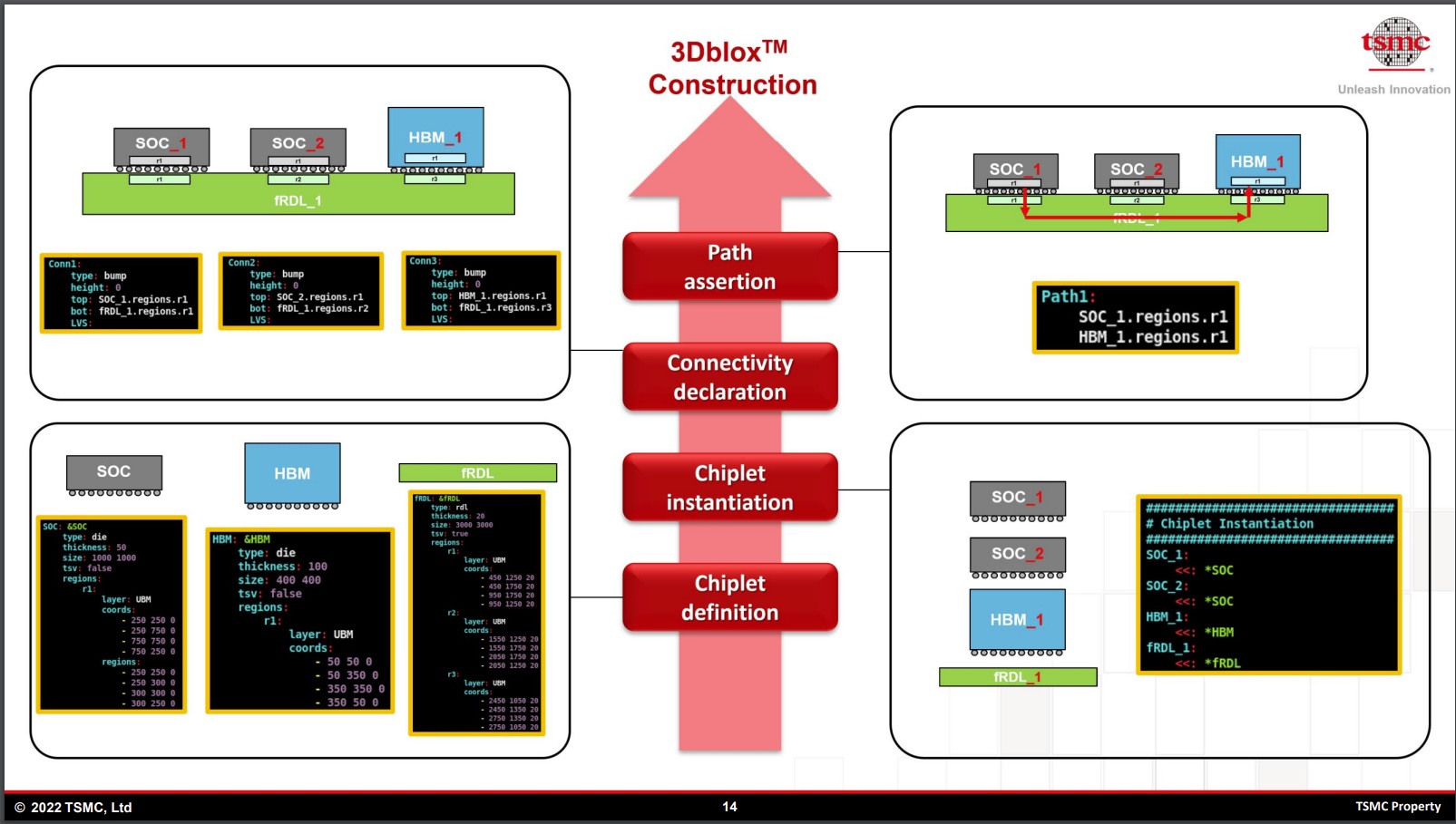
The other interesting announcement was 3Dblox. Dan Kochpatcharin, the new Head of Design Infrastructure Management Division at TSMC, presented the new Open 3dBlox Standard:
TSMC 3Dblox™
To address the rising complexity of 3D IC design, TSMC introduced the TSMC 3Dblox™ standard to unify the design ecosystem with qualified EDA tools and flows for TSMC 3DFabric technology. The modularized TSMC 3Dblox standard is designed to model, in one format, the key physical stacking and the logical connectivity information in 3D IC designs. TSMC has worked with EDA partners in the 3DFabric alliance to enable 3Dblox for every aspect of 3D IC designs, including physical implementation, timing verification, physical verification, electro-migration IR drop (EMIR) analysis, thermal analysis, and more. TSMC 3Dblox is designed to maximize flexibility and ease of use, offering ultimate 3D IC design productivity.

Again, we will cover this in more detail after the virtual event so stay tuned.
Also Read:
TSMC 2022 Open Innovation Platform Ecosystem Forum Preview
Future Semiconductor Technology Innovations
TSMC 2022 Technology Symposium Review – Advanced Packaging Development
Share this post via:


