By Kelly Damalou and Matt Commens
Innovation in semiconductor design today is energized primarily by AI/ML, data centers, autonomous and electric vehicles, 5G/6G, and IoT. Recently developed 2.5 and 3D-IC silicon-based packaging technologies have advanced the state of the art beyond SoC technologies which first united digital, analog, and memory functions on a single chip in the ’90s. These cutting-edge packaging technologies have delivered an effective rebirth of Moore’s Law which had slowed in recent years from limitations to transistor feature size due to thermal and quantum effects in the silicon.
Achieving the desired increase in functionality and performance requires overcoming a set of technical, design, and manufacturing challenges. What were once PCB scale problems are now squeezed into a single stacked or interconnected device, resulting in the desired smaller form factor and potential increases in performance but with accompanied challenges in signal and power integrity along with thermal and mechanical effects. The combination of these challenges ultimately necessitates the use of multiphysics modeling and simulation.
Interposers are a new approach to IC packaging and are often designed and manufactured in a silicon process. Interposers are viewed as a critical path forward for delivery of 3D-IC technology and are currently an area of intense activity in design and simulation. Among the virtues of using silicon as a substrate are its amenability to supporting standard chip features such as metal traces and vias and, as opposed to organic technologies, its thermal match with the die potentially resolves many thermal problems.
There are several numerical techniques for solving the electromagnetics of interposers and 3D-ICs. By far, the most general-purpose technique in electromagnetics is the finite element method (FEM). FEM is used broadly and successfully due to its flexibility in both CAD, material handling, and ready applicability to multi-physics solutions. And when combined with physics driven automatic adaptive meshing, FEM delivers accurate and reliable solutions. With this, FEM has been applied on the fine features of chip scale onto package, PCB, and antenna, and when extended with advanced solver technologies such as the domain decomposition method (DDM) applied on elastic high-performance computing (HPC) hardware, all the way up through large systems. Furthermore, FEM can be hybridized with other large-scale techniques such as the Method of Moments (MoM) or shooting and bouncing rays (SBR).


Fig. 1: Full system in FEM: EMI/EMC study from chip-package-phone-car-chamber.
On-chip electromagnetic extraction has used quasi-static solvers which return RC (resistance, capacitance) SPICE format models. These solvers can be attractive because of their speed and model outputs easily consumable by circuit solvers. However, their discrete RC output ignores inductance and has limited frequency bandwidth and is thus only applicable at relatively small geometric sizes. As the size grows, full wave effects become important, examples being planar on-chip spiral inductors and baluns where amplitude and phase difference need to be considered. A common solver in this regime is the Method of Moment (MoM). MoM can be efficient under the assumption of very thin metal layers on dielectric with infinite extents. However, these assumptions break down as feature sizes have shrunk and the metal layers no longer appear thin and 2D but 3D in their proximity to neighboring conductors. In this “3D regime” the 1D and 2D elements deployed by MoM struggle to adequately capture the coupling impacts from neighboring conductors on the same or adjoining layers which impacts the flow of electrons. This directly affects the trace self and mutual capacitances and inductances which are important to accurate quality factor, Q. Methodologies such as Fast Multipole Method (FMM) ignore the coupling of elements that sit far away from each other in order to improve speed and capacity of MoM, but this compromised calculation of the weak coupling is problematic. On the other hand, PEEC-RWC calculates the coupling among all mesh elements, therefore can very accurately predict the weak coupling even at the highest frequencies.
Turning to silicon-based interposers, by the nature of their design, purpose, and manufacturing they lie in a physical regime where a quasi-static RLC model will not have enough bandwidth, a MoM solver will suffer accuracy issues and be inefficient under the interposer’s 3D nature, and where the general-purpose rigor of FEM may not be necessary. Here a set of coupled techniques known as partial element equivalent circuit (PEEC) and random walk capacitance (RWC) can together extract, in a very efficient fashion, highly accurate full-wave electromagnetic models.

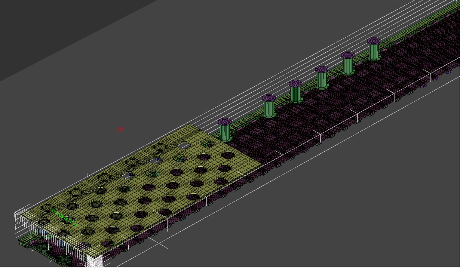
Fig. 2: PEEC mesh of interposer with 48 signal lines and power delivery network.
PEEC-RWC achieves this performance through the generation of a distributed RLCk model which, through advanced HPC-enabled model order reduction (MOR) techniques, can extract a full-wave model very quickly. In addition, it is possible to extend PEEC-RWC to handle layout dependent effects (LDE) prevalent at the small feature size of modern semiconductor processes. And PEEC-RW is by no means limited to solving interposers, it can also model discrete components like spiral inductors and baluns in a similarly efficient fashion. Plus, discrete device modeling is not limited to a single or a few components. PEEC-RW solvers can execute a fully coupled simulation across multiple devices at a scale such as might be found in a multi-channel RF transceiver.


Fig. 3: RF transceiver with multiple radios in the periphery.
Beyond solver considerations is the user’s ability to employ them effectively. However powerful the solver is, an inability for a user to access the functionality will limit its usefulness. Having platforms that cover multiple workflows like IC or package/PCB/system that cater to the appropriate engineering skills set is vital to allowing these techniques to cover the various industry demands and empower engineers to deliver cutting edge solutions for their markets.
3D-IC will be an exciting and cutting-edge technology for many years. Computational multiphysics is already proving to be an essential part of the various design and verification methodologies and associated EDA tool stacks for developing such devices, and it is joining other advanced technology areas embracing this field of simulation for virtual prototyping of their end user products and systems.
Ansys will be discussing electromagnetic simulation and computational multiphysics for 3D-IC frequently during the coming year. You can join the discussion at the links below. Stay tuned for more information in 2023.
Matt Commens is a senior manager for product management at Ansys.
Kelly Damalou
(all posts)
Kelly Damalou is lead product manager for Ansys’ on-chip electromagnetic simulation portfolio.
- Coinsmart. Europe’s Best Bitcoin and Crypto Exchange.Click Here
- Platoblockchain. Web3 Metaverse Intelligence. Knowledge Amplified. Access Here.
- Source: https://semiengineering.com/the-computational-electromagnetics-simulation-challenge-of-3d-ic/

