Test, metrology, and inspection are essential for both the lab and the fab, but fusing them together so that data created in one is easily transferred to the other is a massive challenge.
The chip industry has been striving to bridge these separate worlds for years, but the economics, speed, and complexity of change require a new approach. The never-ending push toward smaller, better-defined architectures drives the need for highly innovative and increasingly complex process control solutions that improve yields, reduce costs, and accelerate time to market. Many of these solutions are initially developed in laboratory settings, and successfully integrating them into both R&D and high-volume manufacturing (HVM) environments is critical for achieving these goals.
Since established fabrication lines are carefully tuned, however, any new test or process variation must carefully address automation, material handling, results reporting, and throughput requirements of a production environment.
“Fabs are, by definition, conservative,” says John Sturtevant, senior director of product development at Siemens EDA. “Once they are running and have an established yield, the rule is don’t touch anything.”
However, as architectures shrink and new IC materials and processes are developed, new and faster metrology and process solutions that help increase yield, improve profits, or meet new industry standards, must also be added. That is a complex undertaking.
“Moving a new tool into a fab can be challenging because customers either have an existing process they use, or they choose to skip a metrology step because the process is stable enough,” says Juliette van der Meer, product manager for Bruker. “Their systems are carefully tuned, and they don’t want to disrupt that. Now, however, especially with automotive, we see regulations for metrology validation getting tighter and tighter for safety reasons. That requires fabs to implement these metrology tools, but it takes time and it can be a major process. It’s a big thing.”
Transitioning lab technologies to the fab often requires a complete redesign of the hardware architecture. This includes new algorithms, powerful servers for analyzing large data streams, and innovative approaches to hardware integration. Careful consideration is required to ensure the tool’s performance aligns with fab requirements while maintaining compatibility with existing processes.
“Fab managers and process development managers are very cost-conscious,” says Sturtevant. “That’s not ever going to change. They go to work each day wondering how to get a half-point increase in yield, or how to get a 10% shrink on a certain process to help lower costs, and there’s not just one bullet. There are lots of little things, and it may be that if you can get 5% improvement in one process window and 2% in another. Then it adds up. The trouble is, it’s all going to cost money. There’s not going to be any solution that’s completely free.”
In other cases, it may require entirely new approaches that have never been used in the fab. This is especially true for 5G millimeter wave chips, which require over-the-air testing in the lab to ensure they are working properly, but that doesn’t easily translate to the fab.
“Over-the-air testing in the lab is quite well-understood,” said Chen Chang, senior director for strategic business development at National Instruments. “You can do more characterization of different materials, and with beamformers the antenna modules can have a big effect on performance. Those are getting packed into the handset, so if people put their hands on top of those antenna modules, it will have a big effect. That’s being well characterized inside the lab environment, all the way through certification and test, and over-the-air tests are critical. Once they move to the production side, over-the-air testing requires a chamber that is quite costly, so many chipset vendors are utilizing a lot of self-calibration technology. They self-calibrate the modules inside of the phones and the real-world environment to make them more flexible. But this also puts a lot more burden on the validation testing.”
Sometimes, the differences between lab and fab are less about technology than they are about context. The parameters used to characterize a process in a lab may not accurately reflect the realities of available data from the fab.
“I would say that’s a big headache,” says Randy Fish, director of product line management for the Synopsys EDA Group. “For the newer stuff, customers are telling us it’s hard to figure out what a Vmin is for a part, so they leave a lot of power on the table by setting it too high. We get aging models right from the foundries, and everybody characterizes with the aging models, and that’s good. But one of the big assumptions is the workload. There has to be some sort of mission profile that you make assumptions on when you characterize. If the actual activity factors aren’t what you estimated, and the environmental conditions are not going to be what you thought they were going to be, then that can produce a result where a part either doesn’t have enough Vmin margin or has too much margin left in.”
It is imperative, therefore, for labs to demonstrate tangible benefits and cost savings to gain buy-in from fabs. But convincing fab managers and process development managers of the benefits and value of these new technologies can be a daunting task. The value proposition must include tangible, measurable benefits provided by the new solution, like achieving tighter control over the manufacturing process, saving precious time, or responding to emerging challenges in real-time.
Meeting the fab challenges
The first challenge in moving a tool from a lab to a fab lies in automating the technology to seamlessly integrate it into the fab environment. This involves the development of robust hardware and software infrastructure, efficient handling mechanisms, recipe-driven processes, calibration standards, and automated calibration procedures.
“In a lab, you often work with coupons, and you place them manually,” says van der Meer. “So, the first challenge is how to handle full wafers. It’s all about engineering, hardware changes, choosing a proper wafer handler, and automating a process that was done manually in a lab. These are challenges that you don’t have in a lab and it takes time to develop and optimize the whole flow and the software and the measurement setup.”
Automating the technology, however, is just the initial step toward making a new metrology solution suitable for a fab. Attention also must be given to fab connectivity and establishing robust process control. Fab connectivity ensures smooth communication and data transfer between different tools and systems within the fab environment. This connectivity is essential for effective process control and coordination. In addition, achieving tool matching to nanometer levels and maintaining stability across varying environmental conditions are crucial for ensuring the reliable and consistent performance of the tool.
Another challenge involves enhancing the performance of the new solution to meet the demanding needs of the production environment. A manual process that takes several days in a lab offers the privilege of making small adjustments in real time to achieve the greatest results. That freedom disappears in a highly automated setting where results are expected in minutes, or even seconds.
“If an OEM or contract manufacturer wants to decrease the beat rate of an SMT line, they can simply buy another pick and place machine because it’s almost always the bottleneck,” says Tim Skunes, R&D director at Nordson’s CyberOptics business unit. “If they want to go faster, they can buy another pick-and-place machine, and another, and so on, until very soon there’s 10 of them in a row. But they’re still only going to buy one inspection system. So those systems better learn to keep up.”
Some of the key improvements necessary for a successful transition to the lab for a new solution include:
- Significantly higher throughput to keep pace with the fast-paced nature of HVM
- Enhancements in accuracy and repeatability to ensure precise measurements and control of critical parameters
- Advanced algorithms and data analysis suites for extracting quantitative information from raw data, enabling comprehensive analysis and decision-making
- Relevant application use cases that showcase the technology’s effectiveness and value in real-world manufacturing scenarios.
“Not only do you need to do the data acquisition at extremely high rate, but also you need to be able to process all that data and generate high-fidelity images,” says Skunes. “So we develop the competence in the algorithms, and I not only want to do that very accurately, I want to do that extremely fast.”
No matter how elegant a solution may be in the lab, however, transitioning it to an R&D or HVM fab is not always warranted or successful. What works well in a lab setting may not work as well in high-volume manufacturing.
“Supporting HVM requirements is a big challenge,” says Frank Chen, director of applications and product management at Bruker Nano Surfaces & Metrology. “If you want to go into a fab environment, there’s a lot of automation to consider with regard to material handling, results reporting, and throughput. What may be fine for a low-volume R&D or lab environment is not appropriate for HVM.”
Furthermore, seamless integration with existing fab infrastructure, robustness across different environmental conditions, and achieving nanometer-level tool matching are essential aspects of making a technology fab-worthy.
“In production, there are requirements for sampling rate, stability, cleanliness, ESD safety, tool-matching, etc.,” Chen says. “Tool footprint is also important since the space inside a fab is quite precious. A ‘Swiss army knife’ approach typical in labs may not be appropriate for fabs, which may want something with a smaller form factor for a very dedicated application. All of those require careful consideration and planning when introducing a new tool or process in the fab.”
Controlling local variation for these new solutions and managing multiple device parameters and properties present additional challenges. Consistency is important for ensuring predictable yields and achieving tight control over the process windows.
“Initially, when you’re just moving directly from lab to fab, you may only have one tool at each site,” Chen explains. “As you deploy fleets where there are multiple tools at the same production site, you have to calibrate all the tools to give the same measurements, within some margin. That needs to be done with both hardware and software calibration to adjust for tool differences, which unfortunately means that you usually de-tune to the lowest-performing tool of the fleet. So you may have tools that are performing hot and are actually better at the measurements, but you have to match your lowest performing tool because they all have to give the same measurements.”
The human element
Automation, connectivity, performance, and consistency represent significant challenges to transitioning a tool from lab to fab, but accounting for the human element is also a critical challenge that must be considered when planning a new integration.
Implementing lab technologies in fabs requires specialized expertise, particularly in areas such as hardware design, software engineering, and algorithm development. Finding the right talent may impact the speed of implementation.
“It can be a challenge to find the right expertise,” says van der Meer. “Good software engineers are scarce for everyone in the industry. In the end, you get it done, but maybe not at the speed that you were hoping for in the beginning.”
Another issue is that because laboratory technicians and process managers for HVM have different concerns, they often use different language regarding new solutions and technologies, which makes communication between the lab and fab more difficult. Finding the right people in both environments to coordinate the integration with the least amount of wasted time is critical.
“You need to get to data that lets you make decisions,” says Thomas Mueller, senior director at Bruker. “It can be very restricting if the operator of such a system needs to be an AFM expert, a physicist with expertise in optics, and an infrared spectroscopist on top of that. This is why it has been a big focus for us to streamline and automate system operation, while ensuring reliable data output, so one can really focus on that data and what it means for the process.”
From lab to fab: AFM-IR and X-ray spectroscopy
Ramping up lab processes that have the benefit of time to the high-speed nature of a fab can negatively impact the value proposition derived from the lab results, unless careful planning and realistic assumptions are included.
A good example of how this can be achieved in a metrology improvement technology that has moved from a lab setting to the R&D fab is Atomic Force Microscopy — Infrared (AFM-IR). Traditional AFM techniques typically suffer from diffraction limits that restrict their spatial resolution to a few micrometers. However, AFM-IR overcomes this limitation by utilizing the AFM tip as a nanoscale IR detector. It combines the topographical information obtained from AFM with the chemical specificity of IR spectroscopy.
“Atomic force microscopy has been in labs and fabs for quite a while,” says Mueller. “But we are seeing increasing levels of adoption for it now with AFM-IR vibrational spectroscopy that offers chemical spectroscopy at the nanoscale. One can now perform FTIR spectroscopy at sub-10nm resolution as opposed to the spatial resolution of 10 microns or so in conventional FTIR. So we are talking about a factor of 1,000 resolution improvement.”
While AFM-IR presents exceptional resolution and non-destructive chemical identification capabilities, moving AFM-IR from lab to fab required significant hardware and software modifications, precise infrared illumination, and sophisticated algorithms. An AFM doesn’t have an infrared light source or infrared optics, so it’s a significant hardware change.
“Our focus is photothermal AFM-IR spectroscopy,” adds Mueller. “One of the beauties of the technique is that the concept and physics are so well understood. Conceptually, a pulsed infrared laser illuminates the sample surface, causing a thermal expansion if an absorber is present. The tip serves as localized detector. That core simplicity leads to interpretable spectra, i.e., spectra that correlate extremely well with FTIR libraries.”
Implementing this revised technology requires careful design, customization, and integration of AFM-IR systems specifically tailored to the requirements of the semiconductor fabrication line. Ongoing collaboration between AFM-IR experts and semiconductor process engineers was necessary to address these challenges effectively and ensure successful integration without compromising the existing fabrication processes.
Despite these issues, the valuable insights provided by AFM-IR into material composition at sub-10nm spatial resolution, are helping fabs detect critical failures and improve overall product quality. That translates into higher yields, lower costs, and increased profits.
“AFM-IR lets you find out what is under the tip, its chemical nature. The method is non-destructive, too,” adds Mueller. “If a device on your wafer is impacted by a nano-contaminant left over from a prior process, you can place that whole wafer in the system. The wafer does not need to be destroyed. Even if it is sub-100nm laterally and as thin as a nanometer, the system has the sensitivity and resolution to obtain an infrared spectrum of that contaminant that you can correlate with an FTIR library.
Figure 1 (below) shows how AFM-IR works. First, a sample is prepared, which may consist of thin films, surfaces, or nanostructures. An AFM probe with a sharp tip is brought into contact with the sample surface, and the tip acts as an IR detector. An IR laser is focused on the back of the AFM cantilever, heating it and causing it to expand and bend. As the AFM tip scans over the sample surface, it interacts with the IR-absorbing regions of the sample, causing the cantilever to vibrate. These vibrations are measured using the deflection of the laser beam reflected off the cantilever, and an IR spectrum is obtained.
By scanning the AFM tip across the sample, point by point, an IR absorption spectrum can be acquired at each location, generating a high-resolution chemical map of the sample surface. AFM-IR offers several advantages over conventional IR microscopy, including the ability to achieve spatial resolution at the nanoscale level and overcoming diffraction limits. It also enables the identification and mapping of chemical components with high spatial resolution, making it useful for studying nanoscale features and defects.
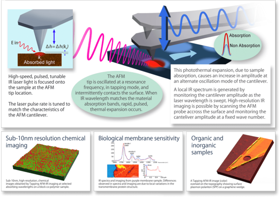
Fig. 1: AFM-IR Process. Source: Bruker
Another example of a successful transition from lab to fab is the recent advancement of X-Ray inspection to automated inline X-ray metrology in HVM production lines.
“X-ray inspection has long been a common failure analysis tool for QA,” says Chen. “3DCT can generate very beautiful images, but it’s a very slow process. Now there is a solution for converting it to a fast, automated inline metrology tool for HVM that helps identify process issues rather than just the defects. This fab solution has never existed before, and customers didn’t know they needed this since they didn’t think it was possible.”
But the implementation was not as simple as attaching a wafer loader or material handler to the tool. It required a complete redesign of the hardware architecture, new algorithms, and more powerful servers for analyzing large data streams.
“There are adoption hurdles, as well,” says Chen. “Fabs are accustomed to using X-ray inspection in a failure analysis lab, which can only look at a few dies and takes a couple of days to turn around results. That’s the visibility they had and what they came to accept as the technology’s capabilities. You need to visualize the defect with 3DCT, which can take hours, and ultimately applications like detecting crack non-wets are resolution-limited by the tool. Now with automated inline X-ray metrology, not only can we detect the defects, we can give a rating system such as automotive grade, industrial grade, consumer grade, etc. Having that visibility and quantity of data gives the confidence to price their products appropriately. Customers want it yesterday, and the effort to bring that from lab to fab requires significant integration work to be compressed into a very short amount of time. We’re going through that crunch right now on some of these applications.”
Conclusion
As the number of process steps increases, along with higher sampling rates and design rule shrinkage, the need for new efficient and high-performing metrology solutions becomes imperative. These solutions must keep pace with the evolving complexity of semiconductor processes to provide accurate measurements and control, but the available time to research and implement these new tools continues to shrink.
The challenges of moving semiconductor manufacturing equipment from a laboratory setting to a fab setting, whether in R&D or HVM, are vast and multi-faceted. From time constraints and metrology cycle times to complex device structures and controlling new materials, each aspect requires innovative solutions and a meticulous transition process. By leveraging long-term research, investigating existing lab technologies, and addressing technological and adoption challenges, the semiconductor industry can continue to meet the ever-increasing demands of advanced technology nodes.
- SEO Powered Content & PR Distribution. Get Amplified Today.
- PlatoAiStream. Web3 Data Intelligence. Knowledge Amplified. Access Here.
- Minting the Future w Adryenn Ashley. Access Here.
- Buy and Sell Shares in PRE-IPO Companies with PREIPO®. Access Here.
- Source: https://semiengineering.com/from-lab-to-fab-increasing-pressure-to-fuse-ic-processes/

