Plasma etching is perhaps the most essential process in semiconductor manufacturing, and possibly the most complex of all fab operations next to photolithography. Nearly half of all fab steps rely on a plasma, an energetic ionized gas, to do their work.
Despite ever-shrinking transistor and memory cells, engineers continue to deliver reliable etch processes.
“To sustainably create chips with nanoscale-level precision and the right cost structure, wafer fab equipment makers need to push the boundaries of plasma physics, materials engineering and data science to deliver the equipment solutions needed,” said Thomas Bondur, corporate vice president for Etch Product Group marketing at Lam Research. Nowhere is this more evident than in plasma etching, which works hand-in-hand with lithography to create exacting, repeatable features on wafers.
This report examines key etch steps in 3D NAND, DRAM, nanosheet FETs, and interconnects, with a forward look at 2D devices and low-budget back-end processing. The industry also is pursuing more sustainable etching chemistries to reduce equivalent CO2 emissions from its fabs.
For many toolmakers, process modeling plays a pivotal role in etch process development. The goal is to shorten time to market while reducing wafer and mask costs.
“Etch process optimization on some of the trickiest steps can take a year or more to complete,” said Barrett Finch, senior marketing director at Lam Research. “We recently completed some process simulation work in three weeks that was expected to take three months using typical silicon-based testing and development.”
This can amount to hundreds of thousands, or even millions of dollars, just for the mask and wafer costs for a device manufacturer.
Etching basics
The etch process works hand-in-hand with lithography. Etching typically is preceded by deposition of a film (by epitaxy, chemical or physical vapor deposition, etc.). Typically, a CVD film is coated with photoresist and then exposed through a patterned reticle (mask) using optical lithography (248nm or 193nm UV, 13.5nm EUV). Resist development then reveals the pattern. In a single wafer plasma etch chamber, typically the etching chemicals and ions bombard and remove the CVD film where the photoresist is missing (in positive tone resist). Following etch, resist ashing, wet chemical cleaning, and/or wet etching remove residues.
Plasma etching processes can be roughly grouped as dielectric, silicon or conductor etches. Dielectrics such as silicon dioxide and silicon nitride are best etched using fluorinated gases while silicon and metal layers react best with chlorine chemistries. There are essentially three dry etching modes — reactive ion etching, plasma etching, and sputter etch (ion beam). Etching processes are all about the complex interactions between the chemical reactants, plasma and wafer materials. When RF bias is applied to a reactive gas, electrons and positively charged ions bombard the wafer to physically remove (etch) material while the chemical species and free radicals react with the exposed material to form volatile byproducts. Etching can be either isotropic (reacting equally vertically and horizontally), anisotropic (vertical only) or somewhere in between.
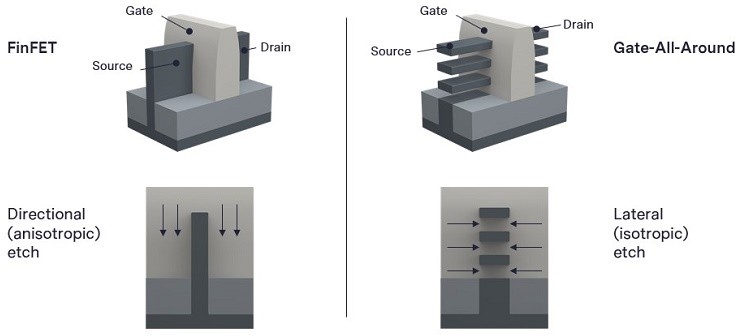
Fig. 1: Transition from finFET to GAA drives critical isotropic selective etch requirements. Source: Lam Research
The metrics etch engineers care most about are etch rate, profile control, uniformity (across the wafer), and etch selectivity, because these affect yield and productivity. Etch selectivity is simply the ratio of removal of the material you want to etch relative to its underlayer – for instance, SiO2 on silicon. During etching, it also is advantageous not to remove too much photoresist. But when that is the case, often the pattern is transferred to a hard mask (silicon dioxide, silicon nitride, SiOC, TiN) before it is transferred to the underlying film.
Selectivity specifications vary from 2:1 on up to 1,000:1 (highly selective etch). With each new node, these specs get tighter. “With high-NA EUV beginning to replace regular EUV within the next four years, the focus is much lower, so you can no longer expose thick photoresist – and by thick I mean 30 nanometers,” said Philippe Bézard, dry etch R&D engineer at imec. “But you still need to pattern the same film thickness below. So now you’re asking for much higher selectivity in the sense that instead of 2:1 we have to reach more like 10:1, which is a sudden 4X to 5X selectivity improvement.”
From proof of concept (POC) to high-volume manufacturing (HVM)
Bézard describes three phases of etch process development:
- Determining what etcher, gases, assist layers, etc., are needed to perform the etch;
- Demonstrating performance at fully removing film within specifications with process uniformity across one wafer, and
- Determining how the process can be repeated across thousands of wafers in HVM with high yield and little drift.
Typically, skilled etch and integration engineers handle the first two phases of development. The third phase might again utilize engineering expertise, but machine learning could assist.
“Machine learning and data analysis in general is only useful in the third phase,” he said. “It’s very powerful because it has access to a ton of data and can make sense of a million tiny, simple things that are all interacting. So for a human brain to try to figure this out is very hard, but it’s more manageable for a computer program. But in cases where you have a new application, new material being etched or a new integration, it’s not showing any improvement over humans.”
ML use also pertains to manufacturing cost because thousands of wafers are used in phase three — at least an order of magnitude larger than are used in phases one and two.
Barrett Finch, senior director of the Etch Product Group at Lam Research, describes new process pathfinding as taking a proof-of-concept from a nominal process flow and layout and developing one or more working devices on a wafer. This POC is then transferred to a product development team in the fab to scale up the process and improve yield.
“The amount of work required to transform a nominal proof-of-concept into a viable yielding product is often underestimated, and this creates a big gap to profitability,” Finch said. “Process window modeling seeks to close this gap by introducing fab variation into the early stages of R&D pathfinding.” He suggests that virtual DOEs and Monte Carlo-based analysis across a number of process parameters tests a POC by simulating expected variability.
“Process window modeling can answer the question, ‘What CD or level of variability do I have to maintain to reach minimum device performance and yield?’ We have completed virtual process window tests with upwards of 1 million virtual wafers in a few days, which would be impossible to accomplish in real life,” he said.
Multiple parameters affect etch rate, profile, and selectivity. A key one is temperature. “The impact of thermal effects in etch processing are seen by our customers as they control etch rates, selectivities, and etched profiles. All of these parameters can impact both device yield and fab productivity,” said Benjamin Vincent, senior manager for semiconductor process and integration engineering at Lam Research. He contends that simulation may be especially helpful when a process step has multiple possible configurations (process space is large), or where the downstream results from the step are highly unpredictable.
“The etch process relies on the surface temperature of the wafer, which depends on several heat fluxes — including thermal conduction, ion impact energies, surface reactions, and plasma radiative heat fluxes,” said Alex Guermouche, product marketing manager at Esgee Technologies, a Lam Research Company. “As a result, plasma models need to incorporate all of these physics features to accurately depict temperature changes on the wafer’s surface. Process simulation software can model a range of etch attributes, allowing us to get a better etch result faster and accelerate the customer’s ability to ramp production or optimize yield.”
Precise timing of the etch process
With tighter geometries and thinner films, there’s a need to balance etch rate with great control over other operating parameters.
“With shrinking design rules, many etch processes are moving to very fast plasma etch process steps that require highly precise control of all reaction inputs: power, pressure, chemistry, and temperature,” said Finch, noting there is also a trend toward optimized plasma pulsing behavior to generate a particular ion-to-neutral ratio, then sweep away by-products. “Advanced modeling of such conditions will be critical to enabling further device scaling.”
Manufacturers of etching systems have been using modeling software for some time to speed next node development or ramp yields. This is no surprise, given the sheer complexity of the process and all its variables.
“There is simply not enough time or enough wafers to execute all possible process experiments when developing next-node technologies,” said Finch. “The number of etch equipment setting combinations can run into the millions, or even billions, and brute force wafer development using all process possibilities is simply impossible.”
Of course, all good models are verified on actual chips. “An accurate model should be predictive, and it should solve the targeted problem that a user wants to solve,” said Finch. “Each time a process or design change has been recommended based upon simulation work, actual fab data should reflect the results of the recommendation. In our case, we have been able to accurately predict the effect of process changes using model-based results, and quickly solve difficult process and technology development problems.”
Tool suppliers also are working on advanced etch processes to more closely integrate lines and transform what was once a two-mask level process (two lithography steps) into one for process simplification and cost reduction.
“Instead of adapting existing hardware to make the Swiss Army knife even more equipped, companies are introducing technologies that are application specific, such as new systems to address tip-to-tip issues,” said Bézard. The aim is to make two lines facing one another closer together, which currently involves a line patterning step followed by a cut mask. “What Applied Materials and others are introducing is a way of directly etching in the horizontal direction.” Such processes also can widen via holes.
Etch steps for nanosheet FETs
The most critical etch steps in nanosheet process flows include the dummy gate etch, anisotropic pillar etch, isotropic spacer etch, and the channel release step. [1] The profile etch through alternating layers of silicon and SiGe is anisotropic and uses fluorinated chemistry. The inner spacer etch (indentation) and channel release step are optimized to remove SiGe with extremely low silicon loss.
The channel release step is critical. “The release of the nanosheet asks for extremely high selectivity,” said Bézard. “Most nanosheets are silicon, then silicon-germanium and silicon. You have alternating layers, and you need to remove one without modifying the other at all.” Some publications have discussed performing a multi-step SiGe etch to reduce stress to the structure induced by a single etch step.
Next in the process is the formation of self-aligned contacts. “Here what we are trying to do is basically etch silicon dioxide and not touch or recess the silicon nitride. Current specs are, let’s say, 3nm of recess, but people are requesting zero loss,” said Bézard. “In this case we are not even using the word selectivity. We just talk about recess – and zero recess at that.”
3D NAND
For 3D NAND flash, the number of layers continues to grow and necessitates the adoption of multiple stacked tiers in the future, eventually creating vertical strings of stacked devices. “Also, there is a lot of drive to scale the word line pitch or vertical/Z-pitch of the layers as the number of layers grows in order to continue increasing the bit density,” said Robert Clark, senior member of technical staff and technology director at TEL. “From a process perspective, etch and deposition processes will need constant improvement to accommodate the ever-higher aspect ratios at ever-smaller critical dimensions that continued scaling requires.”
Clark described future changes. “Looking toward advanced nodes of charge-trap devices with multiple tiers, engineering of the gate stacks will be required to attain shorter gate lengths, more levels per cell, and improved programming efficiency — potentially through the adoption of high-k materials. Higher conductivity channels will likely be required to replace poly-Si channels in the future, as well,” he said.
One of the most critical etches in 3D NAND involves deep etching of about 100nm holes through multilayer oxide-nitride stacks (200+ layers), which can be up to 10µm deep. Imec’s Bézard said this etch step is a particularly expensive one.
“We have a physical phenomenon that occurs, called the differential charging effect,” he said. “In the plasma we have electrons, ions, and neutral species to simplify a lot. Electrons move in every direction, but ions are accelerated perpendicular to the surface. So you have positive charge at the bottom of the hole and negative charges at the top, and you get an electric field that’s trying to repel incoming ions.”
As a result, high power levels are needed to fully etch the trench. “We’re trying to sustain 30 to 50 gigawatts of power without arcing, and so the chuck has to be extremely well polished and well manufactured,” he said.
The deep etches also induce stresses that need to be minimized, especially because multi-tiered NAND fabrication subsequently requires wafer thinning, precise alignment, and hybrid bonding to the next tier.
Other processes
Not all chipmakers produce leading-edge chips that require EUV lithography. Many fabs are extending their 193nm litho and etch processes.
“We have a high temperature SOC material that we’ve recently started introducing, that extends its patterning capability and can withstand higher temperatures, whether it’s used as underlayer for a CVD layer or mask,” said Brian Wilbur, director of semiconductor products diversification at Brewer Science.
BEOL for the tightest metal lines is expected to undergo a dramatic transition from dual damascene integration schemes to subtractive deposition and etching of interconnect other than copper. Here, two metals — ruthenium and molybdenum — have been the most thoroughly developed. However, molybdenum is more likely to oxidize during etching, making it more compatible with dual damascene schemes. Ruthenium is a noble metal so it does not have the same corrosion issues, but it is more costly.
Device structures also are becoming intolerant of edge placement errors. New schemes for self-alignment from layer to layer and between vias and lines will be needed, according to TEL’s Clark. “The first implementations will likely be for things like buried word lines in DRAM, and the small pitch MOL metal layers for logic where there are needs for higher thermal stability as well as lower resistivity or liner-less metals.”
Next-generation developments
Long term, the industry ideally will transition to lower thermal budget back-end processes (closer to 300°C than 400°C) in order to integrate devices into back-end interconnect layers.
“The industry has a real need to start building devices into more layers,” said TEL’s Clark. “That means we need memory and logic devices built within the BEOL at BEOL thermal budgets.”
So far, devices made using semiconducting oxides appear promising, both for integrating memory devices into a logic BEOL flow, or for building CMOS arrays atop the memory array in DRAMs.
Another substantial shift involves the integration of 2D materials, which research houses and leading chipmakers already are beginning to test. Etching processes for materials like tungsten disulfide or molybdenum disulfide are being considered. The films consist of one monolayer of material so developing fab processes to integrate them is extremely challenging.
Sustainability
Chipmakers and materials suppliers are pursuing alternative chemistries to reduce carbon emissions. In etching, the main culprits are fluorinated gases with high global warming potential.
“A reason why you have PFOS (perfluorooctane sulfonic acid), which is problematic, is because the molecule is so stable,” said imec’s Bézard. “Light or chemical reactions in the atmosphere are not sufficient to break it down.”
He said a number of alternative gas mixtures with higher oxygen content are more easily dissociated and have lower GWP. “However, any candidate has to deliver as good or even higher performance to start.”
But sustainability is not particularly an etch or deposition challenge. It’s a holistic industry challenge from lithography through packaging, where the impact of a new material influences the whole of device processing.
Reference
1. K. Derbyshire, “What’s Different About Next-Gen Transistors”, Semiconductor Engineering, October 20, 2022.
Related Stories
Highly Selective Etch Rolls Out For Next-Gen Chips
Manufacturing 3D structures will require atomic-level control of what’s removed and what stays on a wafer.
- SEO Powered Content & PR Distribution. Get Amplified Today.
- PlatoAiStream. Web3 Data Intelligence. Knowledge Amplified. Access Here.
- Minting the Future w Adryenn Ashley. Access Here.
- Buy and Sell Shares in PRE-IPO Companies with PREIPO®. Access Here.
- Source: https://semiengineering.com/etch-processes-push-toward-higher-selectivity-cost-control/

