| Jan 29, 2021 |
| (Nanowerk News) Two-dimensional (2D) semiconductors have emerged during the past decade as extremely promising for future electronic and optoelectronic devices.
|
|
However, to unlock the significant potential of these fragile materials, we must first find a way to protect them in functional devices, while maintaining their key electronic and optical properties.
|
|
A FLEET-led Australian-German collaboration addresses this issue of fragility by providing a high-performance, ultrathin, protective glass coating.
|
|
They report their findings in Advanced Materials (“Ultrathin Ga2O3 Glass: A Large-Scale Passivation and Protection Material for Monolayer WS2“).
|
 |
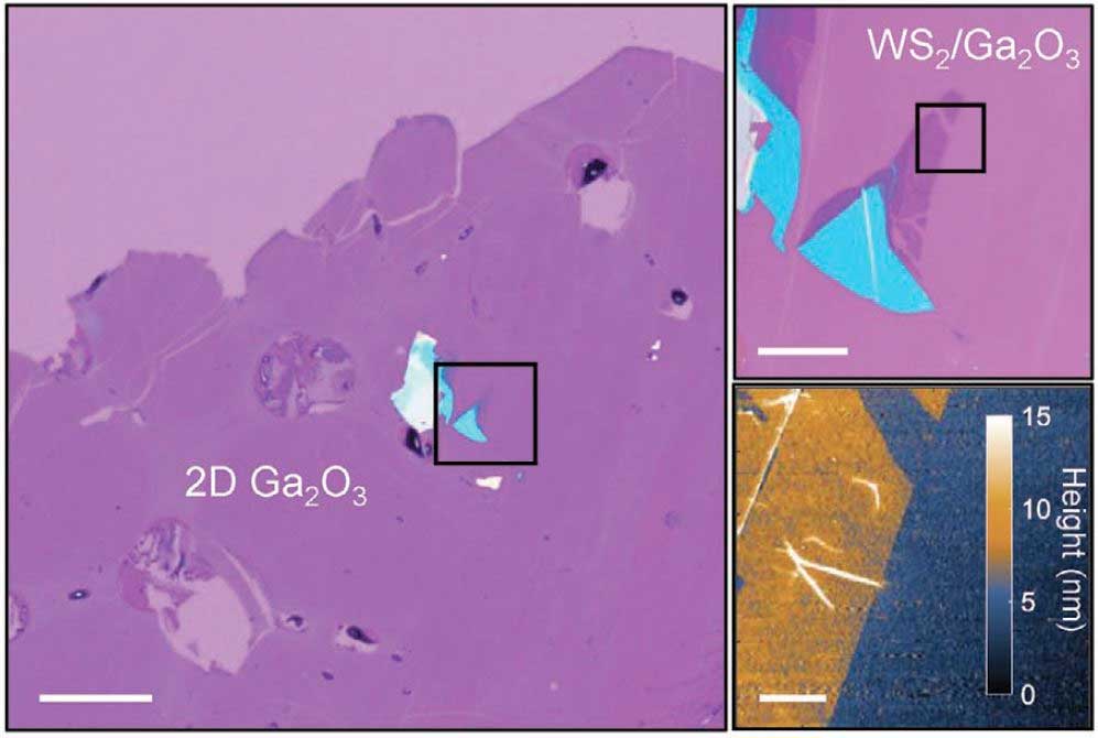
| Tungsten-disulfide / gallium-oxide heterostructure. (Image courtesy of the researchers) (click on image to enlarge)
|
|
The incorporation of 2D semiconductors in multi-layer, solid-state structures on large scales would allow their integration into functional devices, with exciting potential use in compact, ultra-low energy electronics.
|
Wrapping 2D materials in protective, ultrathin glass
|
|
Being only a few layers of atoms in thickness, ‘two dimensional’ materials are inherently fragile.
|
|
To date, the integration of 2D semiconductors into functional devices has been limited by this fragility, or by the scalability of the protective materials being used.
|
|
Thus, we need new methods of protection that are cost-efficient and scalable, while maintaining the material’s necessary electronic and optical properties.
|
|
The new study introduces ultrathin gallium-oxide (Ga2O3) glass as a new, scalable capping material for monolayer tungsten-disulfide (WS2), a key 2D semiconductor.
|
|
With FLEET researchers at ANU, Monash University and RMIT, the new paper describes a novel mechanism for extraordinary protection against deposition of dielectric materials.
|
|
The target material in the new study, tungsten-disulfide, belongs to the group of transition metal dichalcogenide crystals (TMDCs) and is a very promising candidate for various optoelectronic applications functional at room temperature.
|
Why 2D?
|
|
In 2D materials, which might be only one or a few layers of atoms in thickness, the movement of charge-carrying particles (such as electrons) are confined to only two dimensions, and some fascinating quantum effects become predominant.
|
|
For example, some particles moving in two dimensions lose their ability to ‘scatter’, so that electrical resistance vanishes.
|
Source: https://www.nanowerk.com/nanotechnology-news2/newsid=57166.php